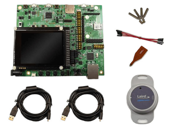
Ezurio DVK-BL5340 Development Kits

Ezurio BL5340 Development Kits provide a platform for rapid wireless connectivity prototyping. These fully featured kits offer the most flexibility for developing BLUETOOTH® Low Energy (LE), 802.15.4, and Near Field Communication (NFC).

The development kit is designed to enable customers to test and validate all the hardware interfaces of the BL5340 module and support the rapid development of application software using either Zephyr RTOS or Nordic Semiconductor nRFConnect SDK. The out-of-box demo for the DVK-BL5340 development board comes pre-loaded, and sample applications are available on the Ezurio Github page.

The Ezurio 453-00052-K1 development kit is for 453-00052 multi-core/protocol Bluetooth + 802.15.4 + NFC module (Nordic nRF5340) with an integrated antenna. The 453-00053-K1 development kit is for 453-00053 multi-core/protocol Bluetooth + 802.15.4 + NFC module (Nordic nRF5340) with a trace pin (ext. antenna).
Features

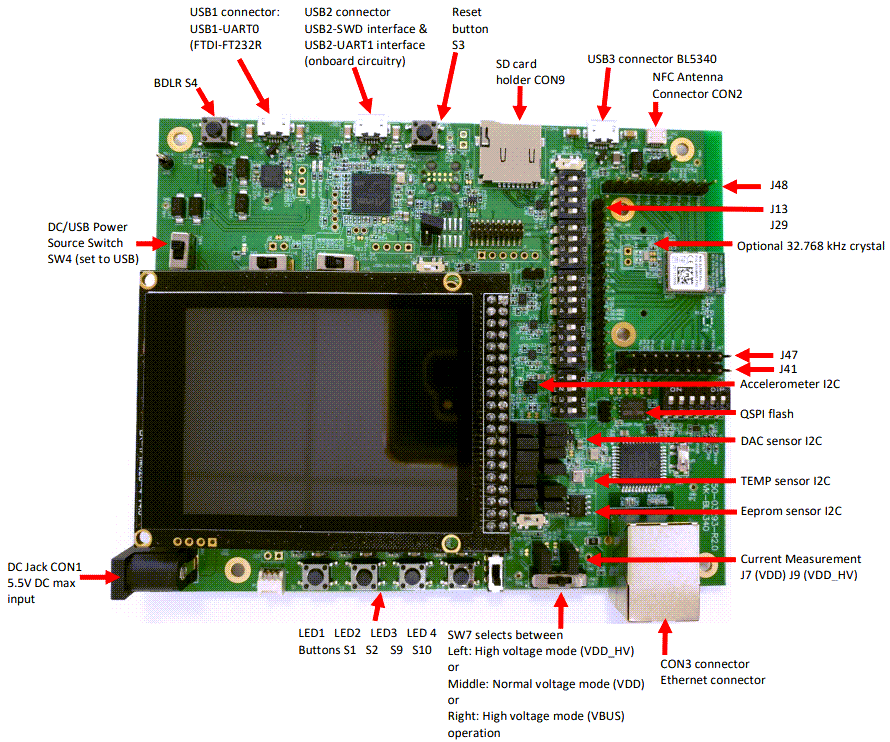
  • BL5340 series module soldered onto the development board
  • The following power supply options for powering the development board
    • USB (micro-USB, type B), either USB1, USB2, USB3 connectors
    • External DC supply CON1(3.5-5.5V) or battery connector (P2)
    • USB3 (micro-USB, type B) –for direct use of BL5340 USB nRF5230 interface as well
  • Powering the BL5340 module in Normal Voltage mode (OPTION1) via selection switch (SW7)
    • Regulated 3.3V or Regulated 1.8V via selection switch (SW5)
  • Powering the BL5340 module in High Voltage mode (OPTION2) via selection switch (SW7)
  • Regulated 2.5V or optional external voltage (from J28 or P2) anywhere between 2.5V to 5.5V for the High Voltage Mode (via J28) via selection switch (SW8)
  • USB1 to UART bridge (FTDI chip, U27)
  • BL5340 can have multiple UARTS; on DVK-BL5340, we have 2 UARTs that can be interfaced to the following
    • USB1 (PC) using the USB-UART0 bridge (U27 FTDI chip)
    • External UART source (using IO break-out connectors J1 (no-pop, plated through holes) when the development board is powered from a DC jack (CON1) or from USB1 (when the jumper is fitted in J35)
    • USB2 (PC) using the Atmel MCU (U14) provided USB2-UART1 bridge (from code running in Atmel U14 chip)
    • Atmel MCU by use of an analog switch to route the BL5340 UART1
      • USB2 (into Atmel MCU U14) to UART1 to connect to the UART1 of the BL6340 (via closed DIP switch S7)
  • Current measuring options (BL5340 module only)
    • Pin header J7, J9 (ammeter)
      • Cut closed solder bridge SB1 to use J7, cut closed solder bridge SB13 to use J9
    • 10R Series resistor for differential measurement (oscilloscope) via open solder bridges
  • IO break-out 2.54 mm pitch pin header connectors (plated through-holes) bring out all GPIO of the BL5340 module – on which various interfaces UART0, UART1, SPI, SPIM4, QSPI, I2C, GPIO, AIN, NFC – and allow for plugging in external modules/sensors
  • Optional external 32.768 kHz crystal (Y3) circuit (Not required for the operation of the BL5340)
    • The 32.768 kHz crystal oscillator circuit requires a load capacitor inside the nRF5340 chipset to be enabled in software (and for the Y3 32.768kHz part, nRF5340 provided load capacitance of 7pF should be used)
    • The Y3 crystal is connected, by default, to the BL5340 by closed solder bridges
  • Optional external serial (QSPI) flash chip (U1)
    • Not required for the operation of the BL5340
    • The closed solder bridges connect it by default
  • Pin headers jumpers or DIP switches that allow the onboard sensors to be disconnected from the BL5340 module (by removing jumpers or DIP switches)
  • Multiple onboard sensors
    • I2C devices
      • 3-axis accelerometer chip (U16) via DIP switch (DIP switch S12 closed by default)
      • Temperature/Pressure/Humidity chip (U5) via 2-pin headers (jumper fitted by default in J3 and J4)
      • EEPROM chip (U2) via 2-pin headers (jumper provided by default in J11 and J6)
      • RTC chip (U16) via 2-pin headers (jumper fitted by default in J17 and J21)
      • DAC chip (U17) via 2-pin headers (jumper provided by default in J5 and J10)
      • Port Expander chip (U31) via 2-pin headers (jumper fitted by default in J16 and J18, J22) on which are connected
        • Four buttons (S1, S2, S9, S10)
        • Four LEDs (LED1, LED2, LED3, LED4)
      • LCD display assembly (on CON4) I2C interface 2-pin headers (jumper fitted by default in J24, J26)
    • SPI devices and High-Speed SPI (SPIM4) device
      • SD card SPI connector (CON9) via 4-pin DIP switch (DIP switch S6 closed by default)
      • Ethernet to SPI chip (U4) via 4-pin DIP switch (DIP switch S5 closed by default)
      • LCD display assembly (plugged into CON4) SPIM4 (High-speed SPIM4) interface level shifted and via DIP switches (DIP switches S8, S11 closed by default)
    • QSPI device (Flash) chip (U1) via closed solder bridges (by default)
  • One reset button S3 (via U25 level shifter)
  • One BOOT button S4 (connected to P1.11 of BL5340)
  • NFC antenna connector (CON2) onboard development board for use with supplied Flexi-PCB NFC antenna
  • Access to BL5340 Serial Wire Debug (SWD) 2-wire interface (JTAG) on P1 or J46 via analog switch U24
  • Onboard SWD (JTAG) programmer circuitry formed by Atmel MCU (U14) that transforms USB2 to SWD interface (which then connects to BL5340 module SWD interface)
  • FW upgrade or application loading HW capability:
    • Via SWD (USB2 to BL5340 SWD) using onboard SWD (JTAG) programmer circuitry (U14 Atmel MCU) on the BL5340 Development Kit
    • Via UART0 (using the U27 FTDI USB1-UART0)
    • Via UART1 (using the U14 Atmel MCH USB2-UART1)

Board Overview

Mechanical Drawing - Ezurio DVK-BL5340 Development Kits

Ezurio DVK-BL5340 Development Kits