Winbond W66BP6NB/W66CP2NQ SDRAM LPDDR4

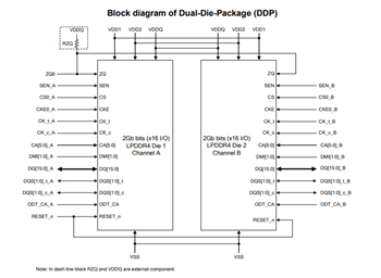
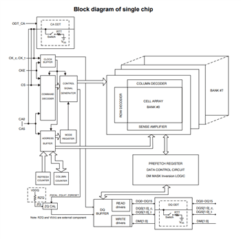
Winbond W66BP6NB/W66CP2NQ SDRAM LPDDR4 offers a Single-Die-Package (SDP) or Dual-Die-Package (DDP) and a 2 or 4 clocks architecture on the Command/Address (CA) bus. The LPDDR4 utilizes the 2 or 4 clocks architecture on the CA bus to reduce the number of input pins in the system. The 6-bit CA bus contains the command, address, and bank information. Each command uses a 1, 2, or 4 clock cycle, during which command information is transferred on the positive edge of the clock.

The Single-Die-Package (SDP) provides 16Mb x 16DQ x 8-banks x 1 channel with 2Gb (2,147,483,648 bits) density. The Dual-Die-Package (DDP) offers 16Mb x 16DQ x 8-banks x 2 channels with 4Gb (4,294,967,296 bits) density.
Features

  • VDD1 = 1.7V to 1.95V
  • VDD2/VDDQ = 1.06V to 1.17V
  • Data width of x16/x32
  • Clock rate of up to 2133MHz
  • Data rate of up to 4267Mbps
  • 8 Internal banks for concurrent operation
  • 16n pre-fetch operation
  • LVSTL_11 Interface
  • Burst length of 16, 32, on-the-fly 16 or 32
  • Sequential burst type
  • Programmable driver strength
  • Coded command input in double clock edges
  • Single data rate architecture on the CA bus
  • Double data rate architecture on the DQ pins
  • Differential clock input
  • Bidirectional differential data strobe
  • Input clock stop and frequency change
  • On-die termination (ODT)
  • Write leveling support
  • Programmable Read and Write Latencies (RL/WL)
  • CA training support
  • DQ-DQS training
  • Refresh features:
    • Auto-refresh (per bank / all bank)
    • Partial array self-refresh
    • Auto temperature-compensated self-refresh
  • Post package repair
  • Target row refresh mode
  • Frequency-Set-Points for fast frequency switch
  • Support write mask and Data Bus Inversion (DBI)
  • Support boundary scan for connectivity test
  • WFBGA 200 Ball (10mm x 14.5mm2) package
  • -40°C ≤ TCASE ≤ 105°C Operating temperature range

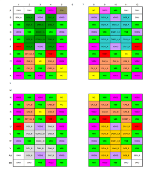
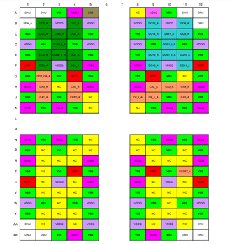
Ball Assignments

Winbond W66BP6NB/W66CP2NQ SDRAM LPDDR4

Winbond W66BP6NB/W66CP2NQ SDRAM LPDDR4

Block Diagrams

Block Diagram - Winbond W66BP6NB/W66CP2NQ SDRAM LPDDR4

Block Diagram - Winbond W66BP6NB/W66CP2NQ SDRAM LPDDR4

Winbond W66BP6NB/W66CP2NQ SDRAM LPDDR4