Transphorm TP65H150BG4JSG 650V SuperGaN® GaN FET

Transphorm TP65H150BG4JSG 650V SuperGaN® Gallium Nitride (GaN) FET is a 650V, 150mΩ normally-off device offering superior quality and performance. TP65H150BG4JSG combines state-of-the-art high-voltage GaN HEMT and low-voltage silicon MOSFET technologies in a 5mm x 6mm PQFN package. Operating within a -55°C to +150°C temperature range, this component features 83W maximum power dissipation, an 10A to 16A maximum continuous drain current range, and a 55A pulsed drain current (maximum). The Gen IV SuperGaN® platform uses advanced epi and patented design technologies to simplify manufacturability while improving efficiency over silicon via lower gate charge, output capacitance, crossover loss, and reverse recovery charge.
Features

  • Gen IV technology
  • JEDEC-qualified GaN technology
  • Dynamic RDS(on)eff production tested
  • Robust design, defined by
    • Wide gate safety margin
    • Transient over-voltage capability
  • Very low QRR
  • Reduced crossover loss
  • Achieves increased efficiency in both hard- and soft-switched circuits
  • Easy to drive with commonly-used gate drivers
  • GSD pin layout improves the high-speed design
  • 5mm x 6mm PQFN package
  • Halogen-free and RoHS compliant

Applications

  • Consumer
  • Power adapters
  • Low power SMPS
  • Lighting

Specifications

  • 650V maximum drain-to-source voltage
  • 800V maximum transient drain-to-source voltage
  • ±10V maximum gate-to-source voltage
  • 2.0V to 2.8V gate threshold voltage range
  • 150mΩ to 307mΩ typical drain-source on-resistance range
  • 2.5µA to 10µA typical drain-to-source leakage current range
  • ±100nA gate-to-source leakage current
  • Typical capacitance
    • 400pF input
    • 37pF output
    • 1.2pF reverse transfer
  • 4.9nC typical total gate charge
  • 1.6nC typical gate-source charge
  • 0.8nC gate-drain charge
  • 35nC output charge
  • 8.3A maximum reverse current
  • 1.2V to 1.7V typical reverse voltage range
  • 83W maximum power dissipation at +25°C
  • Maximum continuous drain currents
    • 16A at +25°C
    • 10A at +100°C
  • 55A maximum pulsed drain current
  • 24ns typical turn-on delay
  • 3.2ns typical rise time
  • 22ns typical turn-off delay
  • 4ns typical fall time
  • 28.3ns typical reverse recovery time
  • -55°C to +150°C operating temperature range
  • +260°C maximum soldering peak temperature
  • Thermal resistance
    • 1.5°C/W junction-to-case
    • 50°C/W junction-to-ambient

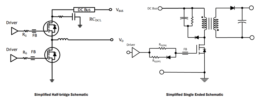
Circuit Implementation

Schematic - Transphorm TP65H150BG4JSG 650V SuperGaN® GaN FET

Transphorm TP65H150BG4JSG 650V SuperGaN® GaN FET