Toshiba TCK42xG Over Voltage Protection Gate Driver ICs

Toshiba TCK42xG Over Voltage Protection Gate Driver ICs are gate drivers designed for external N-channel MOSFETs. These devices support MOSFETs operating in a wide voltage line from 2.7V to 28.0V with various overvoltage lock-out lineups. These devices feature a low standby current, less than 1µA, a built-in charge pump circuit, and MOSFET gate-source protection circuit. The TCK42xG Gate Drivers are suitable for mobile, wearable systems, and power management circuits such as load switch applications. Toshiba TCK42xG Over Voltage Protection Gate Drivers are housed in a small and thin WCSP6G package, ideal for space-constrained applications.
Features

  • Gate driver for N-channel common drain MOSFET
  • Gate driver for N-channel single high side MOSFET
  • VIN max = 40V high maximum input voltage
  • VIN = 2.7V to 28.0V wide input voltage operation
  • VIN_OVLO = 23.26V (Typ.) overvoltage lockout
  • VIN_UVLO = 2.0V (Typ.) under-voltage lockout
  • Gate-source protection circuit
  • Built in Charge pump circuit (gate source voltage VGS = 10V (Typ.))
  • Low standby current – IQ(OFF) = 0.9µA max at VIN = 12V
  • -40°C to +85°C operating temperature range
  • 1.2mm x 0.8mm x 0.35mm WCSP6G package
  • 0.61mg weight

Videos

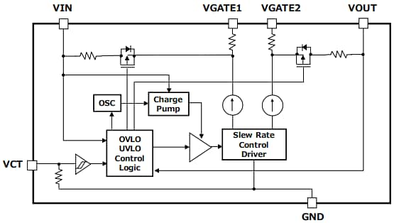
Block Diagram

Toshiba TCK42xG Over Voltage Protection Gate Driver ICs

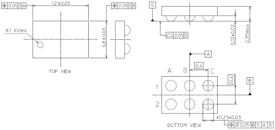
Package Outline

Toshiba TCK42xG Over Voltage Protection Gate Driver ICs

Toshiba TCK42xG Over Voltage Protection Gate Driver ICs