Toshiba TCK12xBG 1A Load Switch ICs

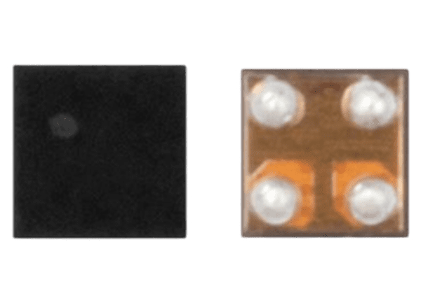
Toshiba TCK12xBG 1A Load Switch ICs are designed for general power management with a slew rate control driver. The TCK12xBG ICs feature ultra-low quiescent current, low switch ON resistance, and a wide 1.0V to 5.5V input operation voltage range. Additionally, the devices provide a quiescent current of 0.08nA and an output current up to 1.0A. Toshiba TCK12xBG 1A Load Switch ICs are housed in a 0.35mm pitch ultra-small WCSP4G package (0.645mm x 0.645mm, t: 0.465mm max.) with a backside coating that protects from external damage. The TCK12xBG ICs are ideal for portable applications that require high-density board assembly and ultra-low power consumption, such as wearables, smartphones, and IoT modules.
Features

  • Wide input operation voltage range of VIN = 1.0V to 5.5V
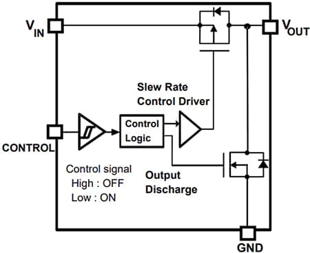
  • Built-in slew rate control driver
  • High output current of IOUT = 1A
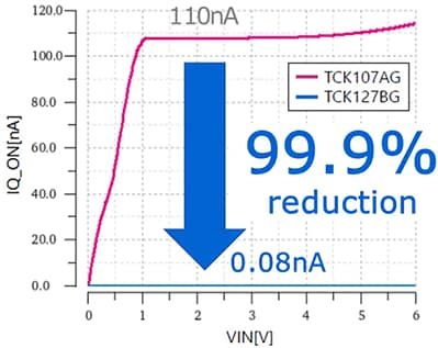
  • Ultra small Quiescent current at IQ = 0.08nA at VIN = 5.5V, VCT = 0V, IOUT =0mA
  • Built in slew rate control driver
  • Low ON resistance
    • RON = 58mΩ (typ.) at VIN = 3.3V, IOUT = -0.5A
  • Low standby current (OFF state) : IQ(OFF)+ISD(OFF)=13nA (typ.)
  • IN (OPR)= 1.0V to 5.5V
  • Built-in auto-discharge (TCK127BG)
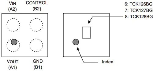
  • Active low (TCK128BG), Active high (TCK126BG, TCK127BG)
  • WCSP4G Ultra small package with back side coating (0.645mm x 0.645mm, t: 0.465mm max.)

Applications

  • Wearables and IoT devices
  • Replacement from load switch circuits formed by discrete semiconductors (MOSFETs, transistors, etc.)
  • Headphones
  • Wireless earbuds
  • Smartphones
  • Smartwatches
  • Streaming devices
  • Smart doorbells
  • AR
  • VR

Videos

Datasheets

  • TCK126BG
  • TCK127BG
  • TCK128BG

Block Diagram

Toshiba TCK12xBG 1A Load Switch ICs

Pin Assignment

Toshiba TCK12xBG 1A Load Switch ICs

Quiescent Current Graph

Toshiba TCK12xBG 1A Load Switch ICs

Toshiba TCK12xBG 1A Load Switch ICs