- support@husseinkey.com
- livechat
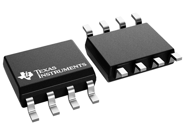
Texas Instruments UCC27624/UCC27624-Q1 Dual-Channel Gate Drivers are high-speed, low-side gate drivers that effectively drive MOSFET, IGBT, SiC, and GaN power switches. The UCC27624/UCC27624-Q1 has a typical peak drive strength of 5A, which reduces the rise and fall times of the power switches, lowers switching losses, and increases efficiency. The device’s fast propagation delay (17ns typical) yields better power stage efficiency by improving the deadtime optimization, pulse width utilization, control loop response, and transient performance of the system.
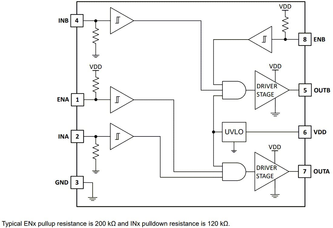
The UCC27624/UCC27624-Q1 can handle –10V at its inputs, which improves robustness in systems with moderate ground bouncing. The inputs are independent of supply voltage and can be connected to most controller outputs for maximum control flexibility. An independent enable signal allows the power stage to be controlled independently of the main control logic. In the event of a system fault, the gate driver can quickly shut off by pulling enable low. Many high-frequency switching power supplies exhibit noise at the gate of the power device, which can get injected into the gate driver’s output pin and cause the driver to malfunction. The device’s transient reverse current and reverse voltage capability allow it to tolerate noise on the gate of the power device or pulse transformer and avoid driver malfunction.
The Texas Instruments UCC27624/UCC27624-Q1 features undervoltage lockout (UVLO) for improved system robustness. When there is not enough bias voltage to fully enhance the power device, the gate driver output is held low by the strong internal pull-down MOSFET.


