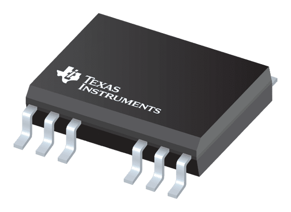
http://www.ti.com/general/docs/suppproductinfo.tsp?distId=26&gotoUrl=https%3A%2F%2Fwww.ti.com%2Flit%2Fds%2Fsymlink%2Fucc21320-q1.pdf%3Fts%3D1591197866″>View Datasheet

Texas Instruments UCC21320-Q1 Isolated Dual-Channel Gate Drivers

Texas Instruments UCC21320-Q1 Isolated Dual-Channel Gate Drivers come with 4A source and 6A sink peak current. They are designed to drive power MOSFETs, IGBTs, and SiC MOSFETs up to 5MHz with best-in-class propagation delay and pulse-width distortion. The input side is isolated from the two output drivers by a 3.75kVRMS basic isolation barrier, with a minimum of 100V/ns common-mode transient immunity (CMTI). Texas Instruments UCC21320-Q1 internal functional isolation between the two secondary-side drivers allows a working voltage of up to 1500VDC.

Every driver can be configured as two low-side drivers, two high-side drivers, or a half-bridge driver with programmable dead time (DT). A disable pin shuts down both outputs simultaneously and allows normal operation when left open or grounded. As a fail-safe measure, primary-side logic failures force both outputs low. Each device accepts VDD supply voltages up to 25V. A wide input VCCI range from 3V to 18V makes the driver suitable for interfacing with both analog and digital controllers. All supply voltage pins have under-voltage lock-out (UVLO) protection. With all these advanced features, the UCC21320-Q1 enables high efficiency, high power density, and robustness.
Features

  • 4A peak source, 6A peak sink output
  • 3V to 18V input VCCI range to interface with both digital and analog controllers
  • Up to 25V VDD output drive supply
  • Switching parameters
    • 19ns typical propagation delay
    • 10ns minimum pulse width
    • 5ns maximum delay matching
    • 6ns maximum pulse-width distortion
  • Common-mode transient immunity (CMTI) greater than 100V/ns
  • Dual low-side, dual high-side or half-bridge driver universal capability
  • Programmable overlap and dead time
  • Wide Body SOIC-14 (DWK) Package
    • 3.3mm spacing between driver channels
  • –40 to +125°C operating temperature range
  • Surge immunity up to 12.8kV
  • Isolation barrier life > 40 years
  • TTL and CMOS compatible inputs
  • Rejects input pulses and noise transients shorter than 5ns
  • Fast disable for power sequencing
  • Qualified for automotive applications
  • AEC-Q100 qualified with the following results
    • Device temperature grade 1
    • Device HBM ESD classification level H2
    • Device CDM ESD classification level C6

Applications

  • HEV and BEV battery chargers
  • Isolated converters in DC-DC and AC-DC power supplies
  • Motor drive and DC-to-AC solar inverters
  • Uninterruptible power supply (UPS)

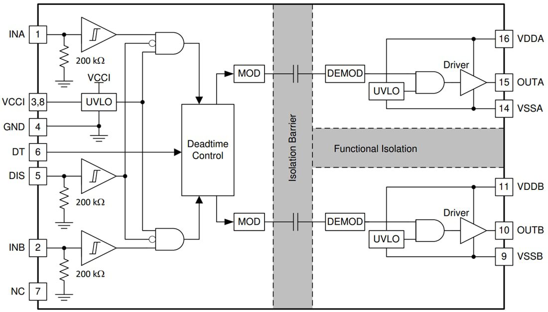
Functional Block Diagram

Block Diagram - Texas Instruments UCC21320-Q1 Isolated Dual-Channel Gate Drivers

Texas Instruments UCC21320-Q1 Isolated Dual-Channel Gate Drivers