http://www.ti.com/general/docs/suppproductinfo.tsp?distId=26&gotoUrl=https%3A%2F%2Fwww.ti.com%2Flit%2Fgpn%2Ftps6593-q1″>View Datasheet

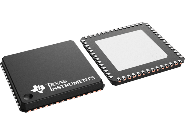
Texas Instruments TPS6593-Q1 Automotive 2.8V to 5.5V PMIC

Texas Instruments TPS6593-Q1 Automotive 2.8V to 5.5V Power Management IC (PMIC) provides four flexible multi-phase configurable BUCK regulators with 3.5A output current per phase and one additional BUCK regulator with 2A output current. All BUCK regulators can be synchronized to an internal 2.2MHz or 4.4MHz or an external 1MHz, 2MHz, or 4MHz clock signal. An integrated spread-spectrum modulation can be added to the synchronized BUCK switching clock signal to improve the EMC performance. This clock signal can also be available to external devices through a GPIO output pin. The device provides four LDOs: three with 500mA capability, which can be configured as load switches, and one with 300mA ability and low-noise performance.

Non-volatile memory (NVM) controls the default configurations and default power sequences, such as GPIO configurations and output voltage. The NVM is pre-programmed to allow start-up without external programming. Most static configurations, stored in the register map of the device, can be changed from the default through I2C or SPI interfaces to configure the device to meet numerous system needs. The NVM contains a bit-integrity-error detection feature (CRC) to stop the power-up sequence if an error is detected, preventing the system from starting in an unknown state. The Texas Instruments TPS6593-Q1 includes a 32kHz crystal oscillator, which generates an accurate 32kHz clock for the integrated RTC module. Backup battery management provides power to the real-time clock (RTC) module and the crystal oscillator from a super-cap or coin cell battery in the event of power loss from the main supply.
Features

  • Qualified for automotive applications
  • AEC-Q100 qualified with the following results
    • The device operates from 3V to 5.5V input supply
    • Device temperature grade 1 (–40°C to +125°C ambient operating temperature range)
    • Device HBM classification level 2
    • Device CDM classification level C4A
  • Functional Safety-Compliant
    • Developed for functional safety applications
    • Documentation to aid ISO26262 and IEC61508 system design will be available upon product release
    • Systematic capability up to ASIL-D and SIL-3
    • Hardware integrity up to ASIL-B and SIL-2
    • Input supply voltage monitor
    • Under/overvoltage monitors and over-current monitors on all output supply rails
    • Watchdog with selectable trigger/Q&A mode
    • Two error signal monitors (ESMs) with selectable level/PWM mode
    • Thermal monitoring with a high-temperature warning and thermal shutdown
    • Bit-integrity (CRC) error detection on internal configuration registers and non-volatile memory (NVM)
  • Low-power consumption
    • 2µA (typ.) shutdown current
    • 7µA (typ.) in backup supply-only mode
    • 20µA (typ.) in low-power standby mode
  • Five step-down switched-mode power supply (BUCK) regulators
    • 0.3V to 3.34V output voltage range in 5mV, 10mV, or 20mV steps
    • One with 4A, three with 3.5A, and one with 2A output current capability
    • Flexible multi-phase capability for four BUCKs: up to 14A output current from a single rail
    • Short-circuit and over-current protection
    • Internal soft-start for in-rush current limitation
    • 2.2MHz/4.4MHz switching frequency
    • Ability to synchronize to external clock input
  • Three low-dropout (LDO) linear regulators with configurable bypass mode
    • 0.6V to 3.3V output voltage range with 50mV steps in linear regulation mode
    • 1.7V to 3.3V output voltage range in bypass mode
    • 500mA output current capability with short-circuit and over-current protection
  • One low-dropout (LDO) linear regulator with low-noise performance
    • 1.2V to 3.3V output voltage range in 25mV steps
    • 300mA output current capability with short-circuit and over-current protection
  • Configurable power sequence control in non-volatile memory (NVM)
    • Configurable power-up and power-down sequences between power states
    • Digital output signals can be included in the power sequences
    • Digital input signals can be used to trigger power sequence transitions
    • Configurable handling of safety-relevant errors
  • 32kHz crystal oscillator with an option to output a buffered 32kHz clock output
  • Real-time clock (RTC) with alarm and periodic wakeup mechanism
  • One SPI or two I2C control interfaces, with a second I2C interface dedicated for Q&A watchdog communication
  • Package option
    • 8mm × 8mm 56-pin VQFNP with 0.5mm pitch

Applications

  • Automotive infotainment and digital cluster, navigation systems, telematics, body electronics and lighting
  • Advanced driver assistance system (ADAS)
  • Industrial control and automation

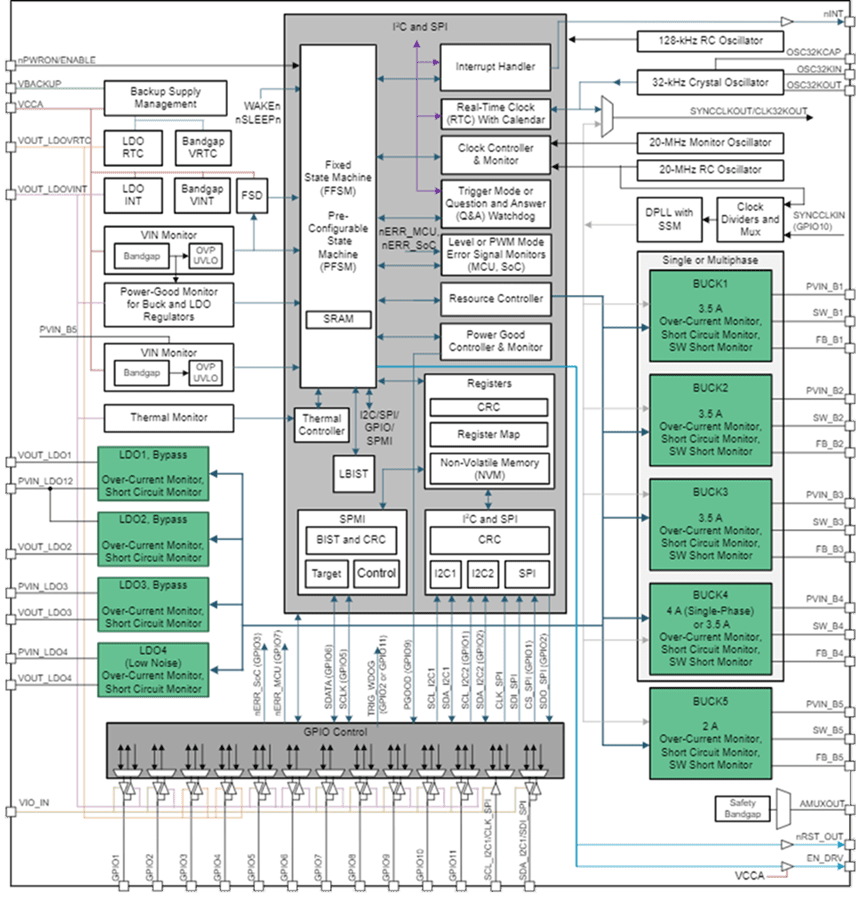
Functional Block Diagram

Block Diagram - Texas Instruments TPS6593-Q1 Automotive 2.8V to 5.5V PMIC

Texas Instruments TPS6593-Q1 Automotive 2.8V to 5.5V PMIC