- support@husseinkey.com
- livechat
http://www.ti.com/general/docs/suppproductinfo.tsp?distId=26&gotoUrl=https%3A%2F%2Fwww.ti.com%2Flit%2Fgpn%2Ftps62870-q1″>View Datasheet
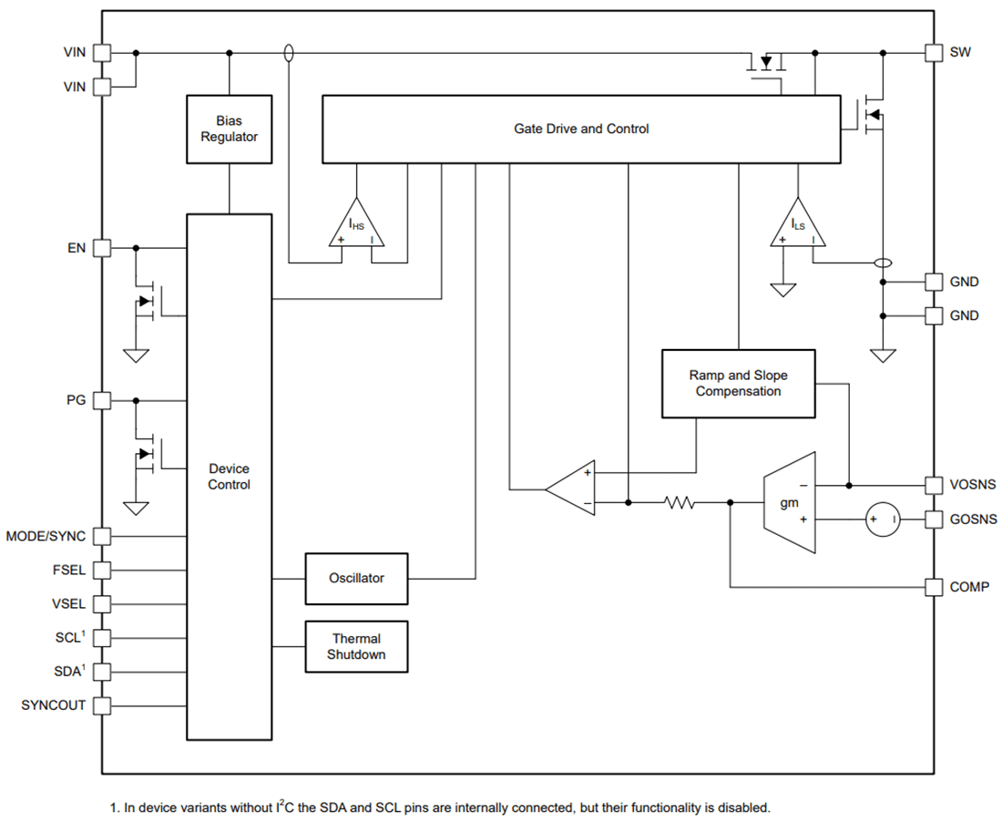
Texas Instruments TPS6287x/TPS6287x-Q1 Synchronous Step-Down Converters are a family of pin-to-pin 6A, 9A, 12A, and 15A step-down DC/DC converters with differential remote sensing. Each current rating offers full-featured device variants with an I2C interface and limited-featured device variants without an I2C interface. All devices provide high efficiency and ease of use. The low-resistance power switches allow up to 15A continuous output current at high ambient temperatures. Each device can operate in a stacked mode to deliver higher output currents. The devices can also be used to spread the power dissipation across multiple devices.
The Texas Instruments TPS6287x/TPS6287x-Q1 family implements an enhanced DCS control scheme that supports fast transients with fixed-frequency operation. Devices operate in power save mode for maximum efficiency or forced-PWM mode for excellent transient performance and have the lowest output voltage ripple. An optional remote sensing feature maximizes voltage regulation at the point of load. The device achieves better than ±1% DC voltage accuracy under all conditions. The switching frequency is resistor-selectable through the FSEL pin. The switching frequency can be set to either 1.5MHz, 2.25MHz, 2.5MHz, or 3.0MHz, or synchronized to an external clock in the same frequency range.
The I2C-compatible interface offers several control, warning, and monitoring features. These include voltage monitoring and temperature-related warnings. The output voltage can be adjusted to adapt the load’s power consumption to the application’s performance needs quickly through the I2C-compatible interface. The default start-up voltage is resistor-selectable through the VSEL pin.


