- support@husseinkey.com
- livechat
http://www.ti.com/general/docs/suppproductinfo.tsp?distId=26&gotoUrl=https%3A%2F%2Fwww.ti.com%2Flit%2Fgpn%2Ftps22999″>View Datasheet
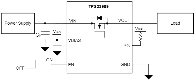
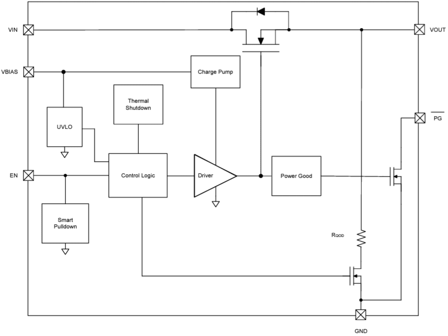
Texas Instruments TPS22999 On-Resistance Load Switch is a single-channel load switch designed to attain a fast turn-on time with a low inrush current. This load switch features an N-channel MOSFET that functions over a 0.1V to VBIAS -1V input voltage range and supports 1.5A maximum continuous current. The TPS22999 load switch integrates a 5.3Ω quick output discharge path while the switch is turned off to enable reliable system operation. This load switch features a Power Good (PG) signal that indicates when the main MOSFET is properly settled to the lowest resistance path. The TPS22999 load switch operates at -40 °C to 105°C free-air temperature range and is available in a 0.35mm pitch and 8-pin WCSP package (YCH). Typical applications include wearables, Solid-State Drives (SSDs), PCs and notebooks, industrial PCs, and optical modules.
