- support@husseinkey.com
- livechat
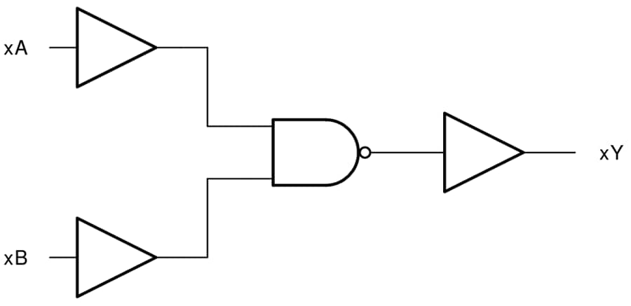
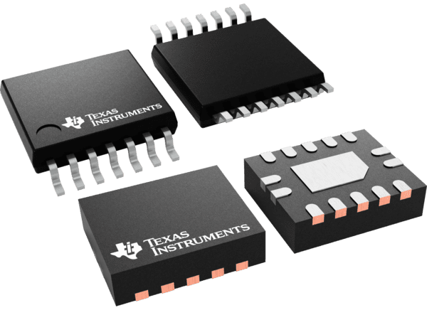
Texas Instruments SN74LV4T00/SN74LV4T00-Q1 Quadruple NAND Gates contain four independent 2-input NAND Gates with Schmitt-trigger inputs. Each gate performs the Boolean function Y = A ● B in positive logic. The output level is referenced to the supply voltage (VCC) and supports 1.8V, 2.5V, 3.3V, and 5V CMOS levels.
The input is designed with a lower threshold circuit to support up translation for lower voltage CMOS inputs (for example, 1.2V input to 1.8V output or 1.8V input to 3.3V output). In addition, the 5V tolerant input pins enable down translation (for example, 3.3V to 2.5V output). The Texas Instruments SN74LV4T00-Q1 devices are AEC-Q100 qualified for automotive applications. The SN74LV4T00-EP devices have gold bond wires, a temperature range of –55 to +105°C, and an SnPb lead finish.


