http://www.ti.com/general/docs/suppproductinfo.tsp?distId=26&gotoUrl=https%3A%2F%2Fwww.ti.com%2Flit%2Fgpn%2Fsn74lv3t98-ep”>View Datasheet

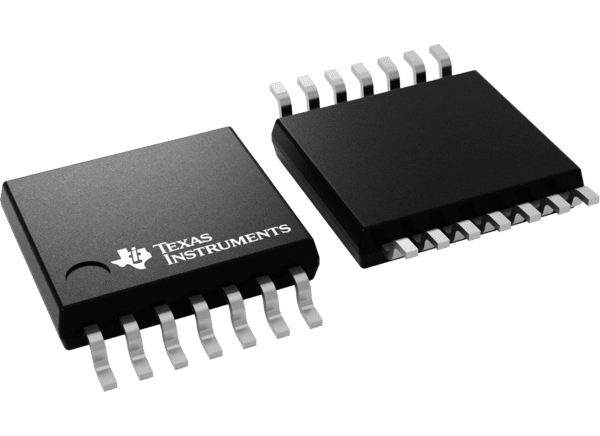
Texas Instruments SN74LV3T98-EP Configurable Multi-Function Gates

Texas Instruments SN74LV3T98-EP Configurable Multi-Function Gates have extended voltage operation to allow for level translation. Eight patterns of 3-bit input determine the output state. Users can choose AND, NAND MUX, NOR, OR, inverter, and non-inverter logic functions. The output level is referenced to the supply voltage (VCC) and supports 1.2V, 1.8V, 2.5V, 3.3V, and 5V CMOS levels.

The input is designed with a lower threshold circuit. This feature supports up translation for lower voltage CMOS inputs (for example, 1.2V input to 1.8V output or 1.8V input to 3.3V output). The 5V tolerant input pins also enable down translation (for example, 3.3V to 2.5V output). The Texas Instruments SN74LV3T98-EP devices have gold bond wires, a temperature range of –55 to +105°C, and an SnPb lead finish.
Features

  • Wide operating range of 1.8V to 5.5V
  • Single-supply voltage translator (refer to LVxT Enhanced Input Voltage)
    • Up translation
      • 1.2V to 1.8V
      • 1.5V to 2.5V
      • 1.8V to 3.3V
      • 3.3V to 5.0V
    • Down translation
      • 5.0V, 3.3V, 2.5V to 1.8V
      • 5.0V, 3.3V to 2.5V
      • 5.0V to 3.3V
  • 5.5V tolerant input pins
  • Supports standard pinouts
  • Up to 150Mbps with 5V or 3.3V VCC
  • Latch-up performance exceeds 250mA per JESD 17
  • Supports defense, aerospace, and medical applications
    • Controlled baseline
    • One assembly and test site
    • One fabrication site
    • Extended product life cycle
    • Product traceability

Applications

  • Enable or disable a digital signal
  • Controlling an indicator LED
  • Translation between communication modules and system controllers

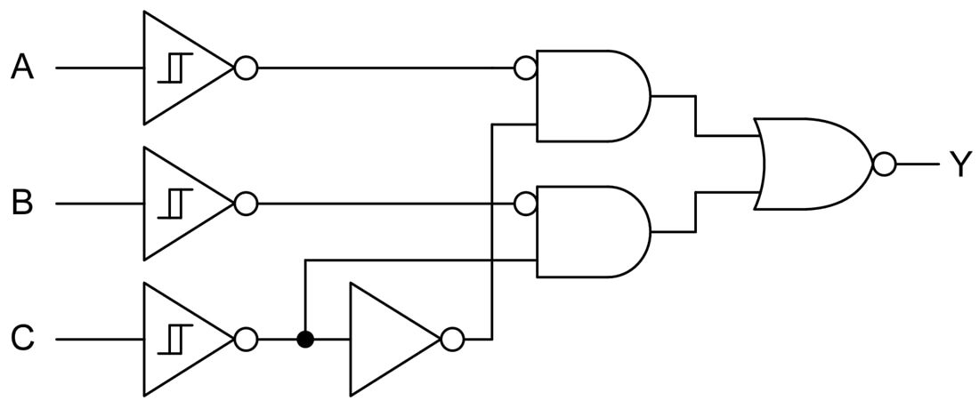
Functional Block Diagram

Block Diagram - Texas Instruments SN74LV3T98-EP Configurable Multi-Function Gates

Texas Instruments SN74LV3T98-EP Configurable Multi-Function Gates