- support@husseinkey.com
- livechat
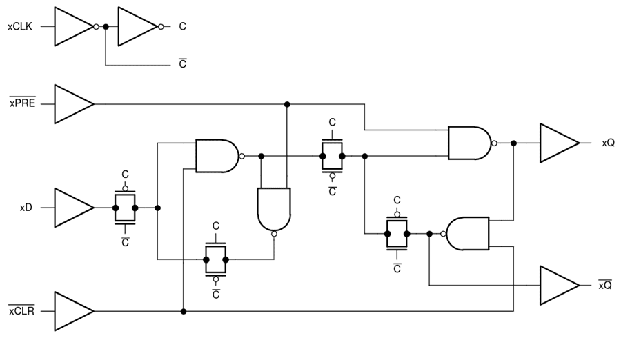
Texas Instruments SN74LV2T74/SN74LV2T74-Q1 Dual D-Type Flip-Flops contain two independent D-type positive-edge-triggered flip-flops. A low level at the preset (PRE) input sets the output high. A low level at the clear (CLR) input resets the output low. Preset and clear functions are asynchronous and not dependent on the levels of the other inputs. When PRE and CLR are inactive (high), data at the data (D) input meeting the setup time requirements is transferred to the outputs (Q, Q) on the positive-going edge of the clock (CLK) pulse. Clock triggering occurs at a voltage level and is not directly related to the rise time of the input clock (CLK) signal. Following the hold-time interval, data at the data (D) input can be changed without affecting the levels at the outputs (Q, Q). The output level is referenced to the supply voltage (VCC) and supports 1.8V, 2.5V, 3.3V, and 5V CMOS levels.
The input is designed with a lower threshold circuit to support up translation for lower voltage CMOS inputs (for example, 1.2V input to 1.8V output or 1.8V input to 3.3V output). In addition, the 5V tolerant input pins enable down translation (for example, 3.3V to 2.5V output). The Texas Instruments SN74LV2T74-Q1 devices are AEC-Q100 qualified for automotive applications. The LSN74LV2T74-EP devices have gold bond wires, a temperature range of –55 to +105°C, and an SnPb lead finish.


