http://www.ti.com/general/docs/suppproductinfo.tsp?distId=26&gotoUrl=https%3A%2F%2Fwww.ti.com%2Flit%2Fgpn%2Fmspm0g3505″>View Datasheet

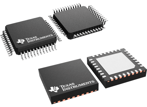
Texas Instruments MSPM0G350x Mixed-Signal MCUs with CAN-FD

Texas Instruments MSPM0G350x Mixed-Signal MCUs with CAN-FD Interface are part of the MSP highly integrated, ultra-low-power 32-bit MCU family. These MSPM0G350x are based on the enhanced Arm® Cortex®-M0+ 32-bit core platform operating at up to 80MHz frequency. The MSPM0G350x MCUs offer up to 128KB embedded flash program memory with built-in Error Correction Code (ECC) and up to 32KB SRAM with hardware parity option. These MCUs provide intelligent digital peripherals such as five general-purpose timers, 16-bit advanced control timers, two windowed-watchdog timers, and one RTC with alarm and calendar modes.

The TI MSPM0G350x MCUs provide data integrity and encryption peripherals (AES, CRC, and TRNG) and improved communication interfaces (four UART, two I2C, two SPI, and CAN 2.0/FD). These MCUs support an extended temperature range of -40°C to 125°C and operate with supply voltages ranging from 1.62V to 3.6V.
Features

  • Core
    • Arm® 32-bit Cortex®-M0+ CPU with memory protection unit, frequency up to 80MHz
  • Operating characteristics
    • Extended temperature of -40°C up to 125°C
    • Wide supply voltage range of 1.62V to 3.6V
  • Memories
    • Up to 128KB of flash memory with error correction code (ECC)
    • Up to 32KB of SRAM with hardware parity
  • High-performance analog peripherals
    • Two simultaneous sampling 12-bit 4Msps analog-to-digital converters (ADCs) with up to 17 external channels
      • 14-bit effective resolution at 250ksps with hardware averaging
    • One 12-bit 1MSPS digital-to-analog converter with integrated output buffer (DAC)
    • Two zero-drift zero-crossover chopper op-amps (OPA)
      • 0.5µV/°C drift with chopping
      • Integrated programmable gain stage, up to 32x
    • One general-purpose amplifier (GPAMP)
    • Three high-speed comparators (COMP) with 8-bit reference DACs
      • 32ns propagation delay in high-speed mode
      • Support low-power mode operation down to 0.7µA
    • Programmable analog connections between ADC, OPAs, COMP, and DAC
    • Configurable 1.4V or 2.5V internal shared voltage reference (VREF)
    • Integrated temperature sensor
    • Integrated supply monitor
  • Intelligent digital peripherals
    • 7-channel DMA controller
    • Math accelerator supports DIV, SQRT, MAC, and TRIG computations
    • Seven timers support up to 22PWM channels
      • One 16-bit general-purpose timer
      • One 16-bit general-purpose timer supports QEI
      • Two 16-bit general-purpose timers support low-power operation in STANDBY mode
      • One 32-bit high-resolution general-purpose timer
      • Two 16-bit advanced timers with deadband support up to 12PWM channels
    • Two window-watchdog timers
    • RTC with alarm and calendar mode
  • Optimized low-power modes
    • RUN: 96µA/MHz (CoreMark)
    • SLEEP: 467µA at 4MHz
    • STOP: 46µA at 32kHz
    • STANDBY: 1.5µA with RTC and SRAM retention
    • SHUTDOWN: 80nA with IO wake-up capability
  • Enhanced communication interfaces
    • Four UART interfaces; one supports LIN, IrDA, DALI, Smart Card, Manchester, and three support low-power operation in STANDBY mode
    • Two I2C interfaces support up to FM+ (1Mbit/s), SMBus/PMBus, and wake-up from STOP mode
    • Two SPIs, one SPI supports up to 32Mbits/s
    • One Controller Area Network (CAN) interface supports CAN 2.0A or B and CAN-FD
  • Clock system
    • Internal 4MHz to 32MHz oscillator with up to ±1.2% accuracy (SYSOSC)
    • Phase-locked loop (PLL) up to 80MHz
    • Internal 32kHz low-frequency oscillator (LFOSC) with ±3% accuracy
    • External 4MHz to 48MHz crystal oscillator (HFXT)
    • External 32kHz crystal oscillator (LFXT)
    • External clock input
  • Data integrity and encryption
    • Cyclic redundancy checker (CRC-16, CRC-32)
    • True random number generator (TRNG)
    • AES encryption with 128 or 256-bit key
  • Flexible I/O features
    • Up to 60GPIOs
      • Two 5V tolerant IOs
      • Two high-drive IOs with 20-mA drive strength
  • Development support
    • 2-pin serial wire debug (SWD)
  • Package options
    • 64-pin LQFP
    • 48-pin LQFP, VQFN
    • 32-pin VQFN
    • 28-pin VSSOP
  • Family members
    • MSPM0G3505: 32KB Flash, 16KB RAM
    • MSPM0G3506: 64KB Flash, 32KB RAM
    • MSPM0G3507: 128KB Flash, 32KB RAM

Applications

  • Motor control
  • Home appliances
  • Uninterruptible power supplies and inverters
  • Electronic point-of-sale systems
  • Medical and healthcare
  • Test and measurement
  • Factory automation and control
  • Industrial transport
  • Grid infrastructure
  • Smart metering
  • Communication modules
  • Lighting

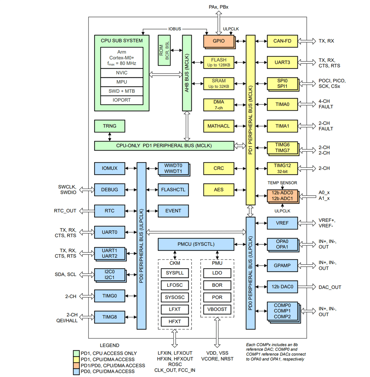
Functional Block Diagram

Block Diagram - Texas Instruments MSPM0G350x Mixed-Signal MCUs with CAN-FD

Texas Instruments MSPM0G350x Mixed-Signal MCUs with CAN-FD