http://www.ti.com/general/docs/suppproductinfo.tsp?distId=26&gotoUrl=https%3A%2F%2Fwww.ti.com%2Flit%2Fgpn%2Flmkdb1120″>View Datasheet

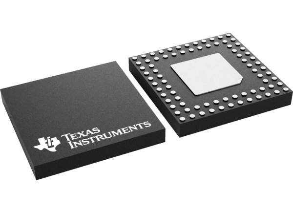
Texas Instruments LMKDB1 Ultra-Low Jitter Clock Buffers

Texas Instruments LMKDB1 Ultra-Low Jitter Clock Buffers are a family of extremely-low-jitter LP-HCSL buffers and MUX that support PCIe Gen 1 to Gen 6 and are DB2000QL compliant. The devices provide flexible power-up sequence, fail-safe inputs, individual output enable and disable pins, loss of input signal (LOS) detection and automatic output disable features, and excellent power supply noise rejection performance. Both 1.8V and 3.3V supply voltages are supported. For the Texas Instruments LMKDB1120, a 1.8V power supply saves 250mW power compared to 3.3V.

Features

  • LP-HCSL clock buffer and clock MUX that support
    • PCIe Gen 1 to Gen 6
    • CC (Common Clock) and IR (Independent Reference) PCIe architectures
    • Input clock with or without SSC
  • DB2000QL compliant
    • All devices meet DB2000QL specifications
    • LMKDB1120 is pin-compatible to DB2000QL
  • Extremely low additive jitter
    • 31fs maximum 12kHz to 20MHz RMS additive jitter at 156.25MHz
    • 13fs maximum additive jitter for PCIe Gen 4
    • 5fs maximum additive jitter for PCIe Gen 5
    • 3fs maximum additive jitter for PCIe Gen 6
  • Fail-safe input
  • Flexible power-up sequence
  • Automatic output disable
  • Individual output enable
  • SBI (Side Band Interface) for high-speed output enable or disable
  • LOS (Loss of Signal) input detection
  • 85Ω or 100Ω output impedance
  • 1.8V/3.3V ±10% power supply
  • -40°C to 105°C ambient temperature

Applications

  • High-performance computing
  • Server motherboard
  • NIC/SmartNIC
  • Hardware accelerator

Typical Application

Chart - Texas Instruments LMKDB1 Ultra-Low Jitter Clock Buffers

Texas Instruments LMKDB1 Ultra-Low Jitter Clock Buffers