http://www.ti.com/general/docs/suppproductinfo.tsp?distId=26&gotoUrl=https%3A%2F%2Fwww.ti.com%2Flit%2Fgpn%2Flmk5c33216a”>View Datasheet

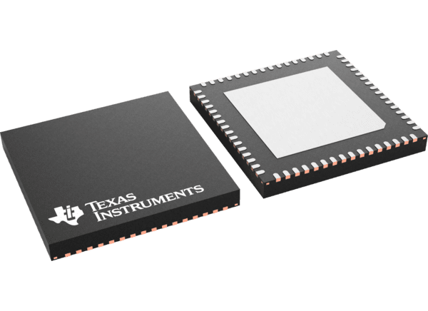
Texas Instruments LMK5C33216A High-Performance Network Synchronizer

Texas Instruments LMK5C33216A High-Performance Network Synchronizer includes a jitter cleaner designed to meet stringent wireless communications and infrastructure application requirements. The network synchronizer integrates three DPLLs to provide hitless jitter and switching attenuation with programmable loop bandwidth and no external loop filters. This feature maximizes the flexibility and ease of use of the device. Each DPLL phase locks a paired APLL to a reference input.

APLL3 features ultra-high-performance PLL with TI’s proprietary Bulk Acoustic Wave (BAW) technology. It can generate 491.52MHz output clocks with 42fs typical/60fs maximum RMS jitter, irrespective of the jitter and DPLL reference input frequency characteristics. APLL2 and APLL1 provide options for a second or third frequency and/or synchronization domain.

Reference validation circuitry monitors the DPLL reference clocks and performs a hitless switch between them upon detecting a switchover event. Zero-Delay Mode (ZDM) and phase cancellation may be enabled to control the phase relationship from input to output. The Texas Instruments LMK5C33216A is fully programmable through the SPI or I2C interface. The onboard EEPROM can be used to customize the system start-up clocks. The device has factory default ROM profiles available as fallback options.
Features

  • Ultra-low jitter BAW VCO based Wireless clocks
    • 42fs typical/60fs maximum RMS jitter at 491.52MHz
    • 47fs typical/65fs maximum RMS jitter at 245.76MHz
  • Three high-performance Digital Phase Locked Loops (DPLLs) with paired Analog Phase Locked Loops (APLLs)
    • Programmable DPLL loop bandwidth from 1mHz to 4kHz
    • < 1ppt DCO frequency adjustment step size
  • Two differential or single-ended DPLL inputs
    • 1Hz (1PPS) to 800MHz input frequency
    • Digital holdover and hitless switching
  • 16 differential outputs with programmable HSDS/LVPECL, LVDS, and HSCL output formats
  • Up to 20 total frequency outputs when configured with 6 LVCMOS frequency outputs on OUT0_P/N, OUT1_P/N, GPIO1, and GPIO2 and 14 differential outputs
    • 1Hz (1PPS) to 1250MHz output frequency with programmable swing and common mode
    • PCIe Gen 1 to 6 compliant
  • I2C, 3-wire SPI, or 4-wire SPI interface
  • –40°C to +85°C ambient operating temperature

Applications

  • 4G and 5G Wireless Networks
    • Active Antenna System (AAS), mMIMO
    • Macro Remote Radio Unit (RRU)
    • CPRI/eCPRI Baseband, Centralized, Distributed Units (BBU, CU, DU)
    • Small cell base station
  • Broadband fixed line access
  • SyncE (G.8262), SONET/SDH (Stratum 3/3E, G.813, GR-1244, GR-253), IEEE 1588 PTP secondary clock
  • Jitter cleaning, wander attenuation, and reference clock generation for 56G/112G PAM-4 SerDes
  • Optical Transport Networks (OTN G.709)
  • Industrial – test and measurement

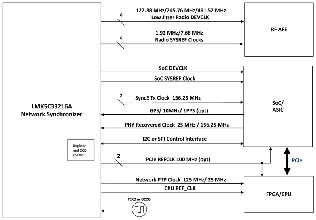
Typical Simplified Block Diagram

Block Diagram - Texas Instruments LMK5C33216A High-Performance Network Synchronizer

Texas Instruments LMK5C33216A High-Performance Network Synchronizer