- support@husseinkey.com
- livechat
http://www.ti.com/general/docs/suppproductinfo.tsp?distId=26&gotoUrl=https%3A%2F%2Fwww.ti.com%2Flit%2Fgpn%2Flmk1d2106″>View Datasheet
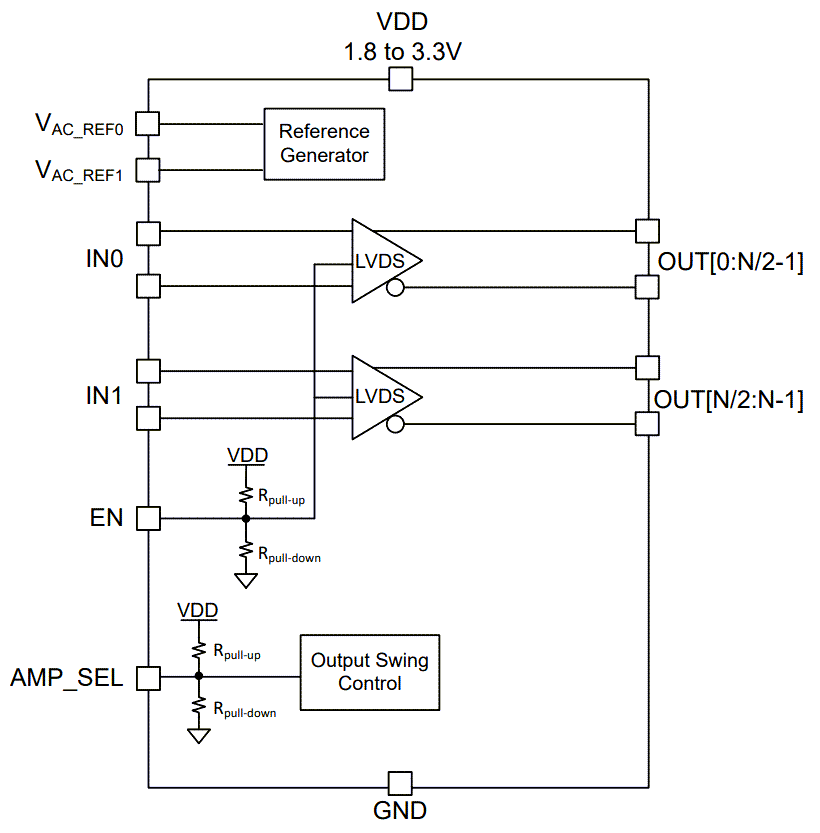
Texas Instruments LMK1D2106/LMK1D2108 LVDS Clock Buffer is specifically designed for driving 50Ω transmission lines. When driving inputs in single-ended mode, apply the appropriate bias voltage to the unused negative input pin. The LMK1D2106 distributes with minimum skew one of two selectable clock inputs (IN0 and IN1) to 12 pairs of differential LVDS clock outputs (OUT0 through OUT11). Similarly, the LMK1D2108 distributes 16 pairs of differential LVDS clock outputs (OUT0 through OUT15). Each buffer block consists of one input and a maximum of 6 (LMK1D2106) or 8 (LMK1D2108) LVDS outputs. The inputs can be LVDS, LVPECL, HCSL, CML, or LVCMOS.
Using the control pin (EN), the Texas Instruments LMK1D2106/LMK1D2108 output banks can either be enable or disabled. If this pin is left open, both bank outputs are enabled. If the control pin is switched to a logic “0”, both bank outputs are disabled (static logic “0”). If the control pin is switched to a logic “1”, the outputs of one bank are disabled while the outputs of the other bank are enabled. The part also supports a fail-safe function. The device further incorporates an input hysteresis which prevents random oscillation of the outputs in the absence of an input signal. The device operates in a 1.8V, 2.5V, or 3.3V supply environment and is characterized from –40°C to 105°C (ambient temperature).


