- support@husseinkey.com
- livechat
http://www.ti.com/general/docs/suppproductinfo.tsp?distId=26&gotoUrl=https%3A%2F%2Fwww.ti.com%2Flit%2Fgpn%2Flmk1d1216″>View Datasheet
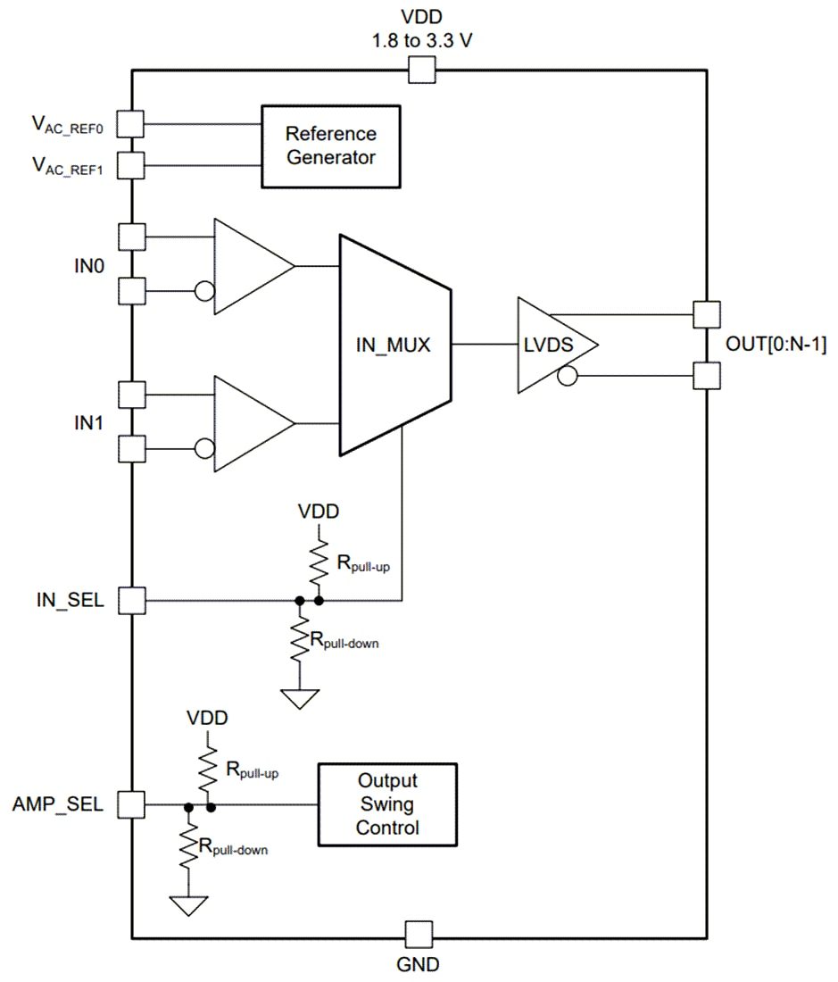
Texas Instruments LMK1D121x Low Additive Jitter LVDS Clock Buffer is specifically designed for driving 50Ω transmission lines. When driving inputs in single-ended mode, apply the appropriate bias voltage to the unused negative input pin. The LMK1D1212 distributes with minimum skew one of two selectable clock inputs (IN0 and IN1) to 12 pairs of differential LVDS clock outputs (OUT0 through OUT11). Similarly, the LMK1D1216 distributes 16 pairs of differential LVDS clock outputs (OUT0 through OUT15). The LMK1D121x family can accept two clock sources into an input multiplexer. The inputs can be LVDS, LVPECL, LP-HCSL, HCSL, CML, or LVCMOS.
The Texas Instruments LMK1D121x IN_SEL pin selects the input, which is routed to the outputs. The part supports a fail-safe input function. The device further incorporates an input hysteresis which prevents random oscillation of the outputs in the absence of an input signal. The device operates in a 1.8V, 2.5V, or 3.3V supply environment and is characterized from –40°C to 105°C (ambient temperature).


