- support@husseinkey.com
- livechat
http://www.ti.com/general/docs/suppproductinfo.tsp?distId=26&gotoUrl=https%3A%2F%2Fwww.ti.com%2Flit%2Fgpn%2Flmk1d1208p”>View Datasheet
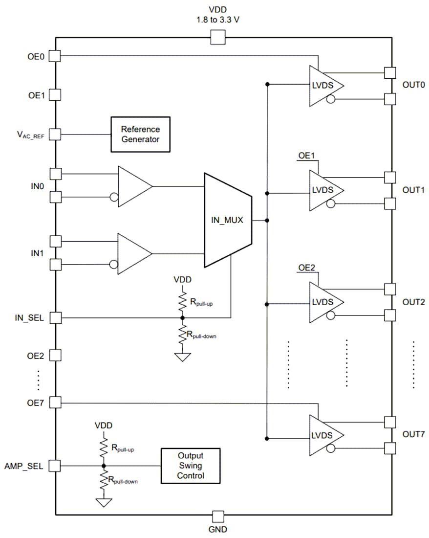
Texas Instruments LMK1D1208P 8-Channel Output LVDS Clock Buffer distributes one of two selectable clock inputs (IN0 and IN1) to eight pairs of differential LVDS clock outputs (OUT0 through OUT7). This distribution is done with minimum skew for clock distribution. The inputs can be LVDS, LVPECL, LVCMOS, HCSL, or CML.
The Texas Instruments LMK1D1208P is specifically designed for driving 50Ω transmission lines. When driving inputs in single-ended mode, apply the appropriate bias voltage to the unused negative input pin. The IN_SEL pin selects the input, which is routed to the outputs. The part supports a fail-safe input function. The device further incorporates an input hysteresis which prevents random oscillation of the outputs in the absence of an input signal.
Each LVDS differential output is enabled by setting the corresponding OEx pin to a logic high 1. If this pin is set to a logic low 0, the output is disabled in a Hi-Z state resulting in reduced power consumption. The device operates in a 1.8V, 2.5V, or 3.3V supply environment and is characterized from –40°C to 105°C (ambient temperature).


