- support@husseinkey.com
- livechat
http://www.ti.com/general/docs/suppproductinfo.tsp?distId=26&gotoUrl=https%3A%2F%2Fwww.ti.com%2Flit%2Fgpn%2Flmk1d1208i”>View Datasheet
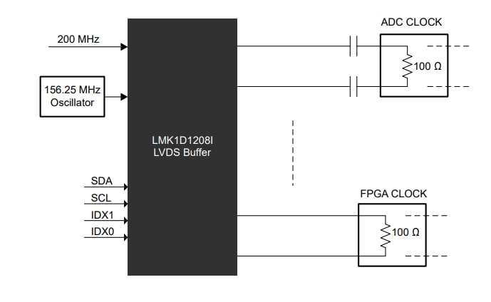
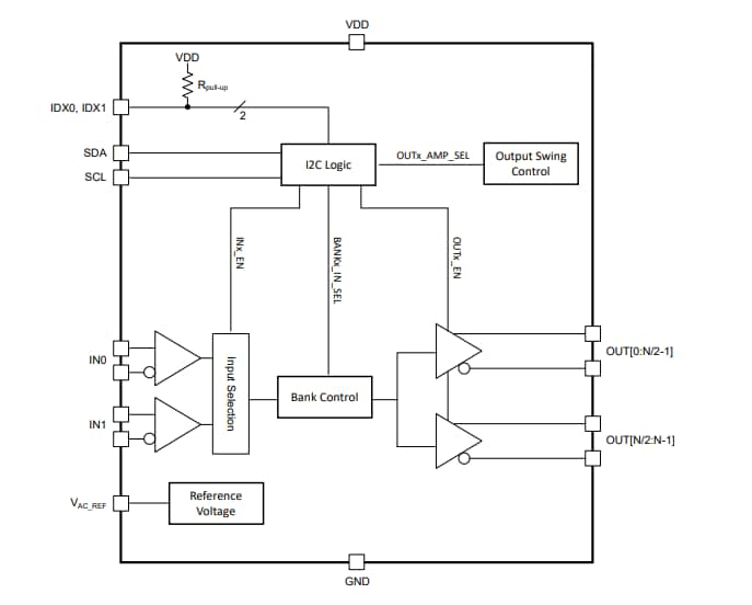
Texas Instruments LMK1D1208I I2C Low-Additive Jitter LVDS Buffers offer two inputs and eight pairs of differential LVDS clock outputs (OUT0 through OUT7) with minimum skew for clock distribution. The inputs allow a choice of either LVDS, LVPECL, LVCMOS, HCSL, or CML.
The TI LMK1D1208I I2C Low-Additive Jitter LVDS Buffers are intended for driving 50Ω transmission lines. Furthermore, when users are driving inputs in single-ended mode, they should apply the appropriate bias voltage to the unused negative input pin. The device’s I2C programming allows configuration as a single bank buffer (one of the two inputs is distributed to eight output pairs) or a dual bank buffer (each input is distributed to four outputs pairs). The LMK1D1208I can configure each output to have either a standard (350mV) or boosted (500mV) swing. The LMK1D1208I combines individual output channel enable/disable through I2C programming. The buffers provide fail-safe inputs that prevent oscillation at the outputs without an input signal and allow for input signals before VDD is supplied.
The LMK1D1208I operates in a 1.8V, 2.5V, or 3.3V supply environment and is distinguished from –40°C to 105°C (ambient temperature).
