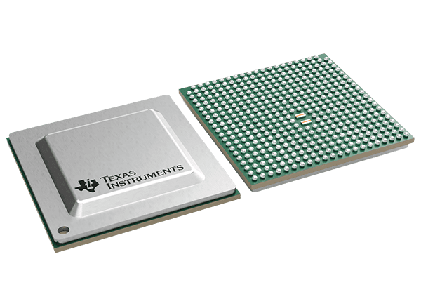
http://www.ti.com/general/docs/suppproductinfo.tsp?distId=26&gotoUrl=https%3A%2F%2Fwww.ti.com%2Flit%2Fgpn%2Fdra821u-q1″>View Datasheet

Texas Instruments DRA821x Jacinto™ 64-Bit Processors

Texas Instruments DRA821x Jacinto™ 64-Bit Processors are based on the Armv8 architecture and are optimized for gateway systems with cloud connectivity. The System-on-Chip (SoC) design reduces system-level costs and complexity through integration—notably, a system MCU, functional safety and security features, and an Ethernet switch for high-speed communication. Integrated diagnostics and functional safety features are targeted to ASIL-D and SIL 3 certification requirements. A PCIe controller and a TSN-capable Gigabit Ethernet switch enable real-time control and low-latency communication.

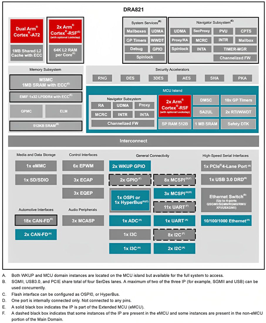
Up to four general-purpose Arm® Cortex®-R5F subsystems can handle low-level, timing-critical processing tasks, leaving the Arm Cortex-A72 core unencumbered for advanced and cloud-based applications. The Jacinto DRA821x processors include the Extended MCU (eMCU) domain concept. This Domain is a subset of the processors and peripherals on the Main Domain targeted at higher functional safety enablement, such as ASIL-D/SIL-3. The functional block diagram highlights which IPs are included in the eMCU.
Features

  • Processor cores:
    • Dual 64-bit Arm Cortex-A72 microprocessor subsystem at up to 2.0GHz, 24K DMIPS
      • 1MB L2 shared cache per dual-core Cortex-A72 cluster
      • 32KB L1 DCache and 48KB L1 ICache per A72 core
    • 4× Arm Cortex-R5F MCUs at up to 1.0GHz with optional lockstep operation, 8K DMIPS
      • 32K I-Cache, 32K D-Cache, 64K L2 TCM
      • 2× Arm Cortex-R5F MCUs in isolated MCU subsystem
      • 2× Arm Cortex-R5F MCUs in general compute partition
  • Memory subsystem:
    • 1MB of On-Chip L3 RAM with ECC and coherency
      • ECC error protection
      • Shared coherent cache
      • Supports internal DMA engine
    • External Memory Interface (EMIF) module with ECC
      • Supports LPDDR4 memory types that comply with the JESD209-4B specification. (No support for byte mode LPDDR4 memories or memories with more than 17-row address bits)
      • Supports speeds up to 3200MT/s
      • 32-bit and 16-bit data bus with inline ECC bus up to 12.8GB/s
    • General-Purpose Memory Controller (GPMC)
    • 512KB on-chip SRAM in the Main Domain, protected by ECC
  • Virtualization:
    • Hypervisor support in Arm Cortex-A72
    • Independent processing subsystems with Arm Cortex-A72, Arm Cortex-R5F with isolated safety MCU island
    • IO virtualization support
      • Peripheral Virtualization Unit (PVU) for low latency high bandwidth peripheral traffic
    • Multi-region firewall support for memory and peripheral isolation
    • Virtualization support with Ethernet, PCIe, and DMA
  • Device security (on select part numbers):
    • Secure boot with secure runtime support
    • Customer programmable root key, up to RSA-4K or ECC-512
    • Embedded hardware security module
    • Crypto hardware accelerators – PKA with ECC, AES, SHA, RNG, DES, and 3DES
  • Functional safety:
    • Functional Safety-Compliant targeted (on select part numbers):
      • Developed for functional safety applications
      • Documentation will be available to aid ISO 26262 and IEC 61508 functional safety system design up to ASIL-D/SIL-3 targeted
      • Systematic capability up to ASIL-D/SIL-3 targeted
      • Hardware integrity up to ASIL-D/SIL-3 targeted for MCU Domain
      • Hardware integrity up to ASIL-D/SIL-3 targeted for the Extended MCU (EMCU) portion of the Main Domain
      • Hardware integrity up to ASIL-B/SIL-2 targeted for the remainder of the Main Domain
      • FFI isolation provided between EMCU and the remainder of the Main Domain
      • Safety-related certification
        • ISO 26262 and IEC 61508 planned
    • AEC-Q100 qualified on part number variants ending in Q1
  • High-speed interfaces:
    • Integrated Ethernet TSN/AVB switch supporting up to 4 (DRA821U4) or 2 (DRA821U2) external ports:
      • One port supports 5Gb, 10Gb USXGMII/XFI
      • All ports support 2.5Gb SGMII
      • All ports support 1Gb SGMII/RGMII
      • DRA821U4: Any single port can support QSGMII (using all four internal ports)
      • Non-blocking wire-rate store and forward switch
      • InterVLAN (Layer3) routing support
      • Time synchronization support with IEEE 1588(annex D,E,F)
      • TSN/AVB support for traffic scheduling, shaping
      • Port mirroring feature for debugging and diagnostics
      • Policing and rate-limiting support
    • One RGMII/RMII port in safety MCU island
  • One PCI-Express Gen3 controller:
    • Gen1, Gen2, and Gen3 operation with auto-negotiation
    • 4× lanes
  • One USB 3.1 Gen1 dual-role device subsystem:
    • Supports type-C switching
    • Independently configurable as a USB host, USB peripheral, or USB dual-role device
  • Automotive interfaces
    • Twenty CAN-FD ports
    • 12× Universal Asynchronous Receiver/Transmitter (UART)
    • 11× Serial Peripheral Interfaces (SPI)
    • One 8-channel ADC
    • 10× Inter-Integrated Circuit (I2C™)
    • 2× Improved Inter-Integrated Circuit (I3C)
  • Audio interfaces:
    • 3× Multichannel Audio Serial Port (McASP) modules
  • Flash memory interfaces:
    • Embedded Multi Media Card ( eMMC™ 5.1) interface
      • Support speeds of up to HS400
  • One Secure Digital 3.0/Secure Digital Input Output 3.0 (SD3.0/SDIO3.0) interfaces
  • One Octal SPI / Xccela™ / HyperBus™ Memory Controller (HBMC) interface
  • 16nm FinFET technology
  • 17.2mm x 17.2mm, 0.8mm pitch, IPC Class 3 PCB

Applications

  • Automotive gateways
  • Vehicle compute
  • Body control module
  • Telematics control unit
  • V2X/V2V
  • Factory automation gateways
  • Communications equipment
  • Industrial transport
  • Building automation gateways

Functional Block Diagram

Block Diagram - Texas Instruments DRA821x Jacinto™ 64-Bit Processors

Texas Instruments DRA821x Jacinto™ 64-Bit Processors