http://www.ti.com/general/docs/suppproductinfo.tsp?distId=26&gotoUrl=https%3A%2F%2Fwww.ti.com%2Flit%2Fgpn%2Fdac12dl3200″>View Datasheet

Texas Instruments DAC12DL3200 12-Bit High-Speed DAC

Texas Instruments DAC12DL3200 12-Bit High-Speed Digital-to-Analog Converter (DAC) is a very low latency, dual-channel, RF sampling DAC. This DAC is capable of input and output rates of up to 3.2GSPS in dual-channel mode or 6.4GSPS in single-channel mode. When using the multi-Nyquist output modes, the DAC can transmit signal bandwidths beyond 2GHz at carrier frequencies approaching 8GHz. The high output frequency range enables direct sampling through C-band (8GHz) and beyond.

The DAC12DL3200 can be used as an I/Q baseband DAC in dual channel mode. The high sampling rate and output frequency range also make the DAC12DL3200 capable of arbitrary waveform generation (AWG) and direct digital synthesis (DDS). An integrated DDS block enables single tone and two-tone generation on-chip.

The Texas Instruments DAC12DL3200 has a parallel LVDS interface that consists of up to 48 LVDS pairs and 4 DDR LVDS clocks. A strobe signal is used to synchronize the interface, which can be sent over the least significant bit (LSB) or optionally over dedicated strobe LVDS lanes. Each LVDS pair is capable of up to 1.6Gbps. Multi-device synchronization is supported using a synchronization signal (SYSREF) and is compatible with JESD204B/C clocking devices. SYSREF windowing eases synchronization in multi-device systems.
Features

  • 12-bit resolution
  • Maximum input and output sample rate:
    • Single-channel up to 6.4GSPS
    • Dual-channel up to 3.2GSPS
  • Multi-Nyquist operating modes
    • Single-channel modes: NRZ, RTZ, RF
    • Dual-channel modes: NRZ, RTZ, RF, 2xRF
  • 6 to 8ns low latency through the device
  • Matching transmit capabilities to the low latency receiver ADC12DL3200
    • DAC and ADC combined latency < 15ns (not including FPGA)
  • Parallel DDR LVDS interface
    • Source synchronous interface to simplify timing:
    • 24 or 48 LVDS pairs up to 1.6Gbps
    • 1 LVDS DDR clock per 12-bit bus
  • > 8GHz output frequency range
  • 21mA full-scale current
  • Simplified clocking and synchronization
    • SYSREF windowing eases setup and hold times
  • On-chip direct digital synthesizer (DDS)
    • Single-tone and two-tone sine wave generation
    • 32 x 32-bit numerically controlled oscillators
    • Fast frequency hopping capability (< 500ns)
    • Synchronous CMOS frequency/phase input
  • Performance at fOUT = 4.703GHz, 6.4GSPS, RF mode
    • –3dBm output power
    • –147dBc/Hz noise floor (70MHz offset)
    • 60dBc SFDR
  • 1.0V, 1.8V, –1.8V power supplies
  • 1.49W (2-ch, RF mode, 3.2GSPS) power consumption
  • 256-Ball FCBGA (17mm x 17mm, 1mm pitch) package

Applications

  • Electronic warfare
  • Generator: pulse, pattern, and arbitrary waveform (AWG)

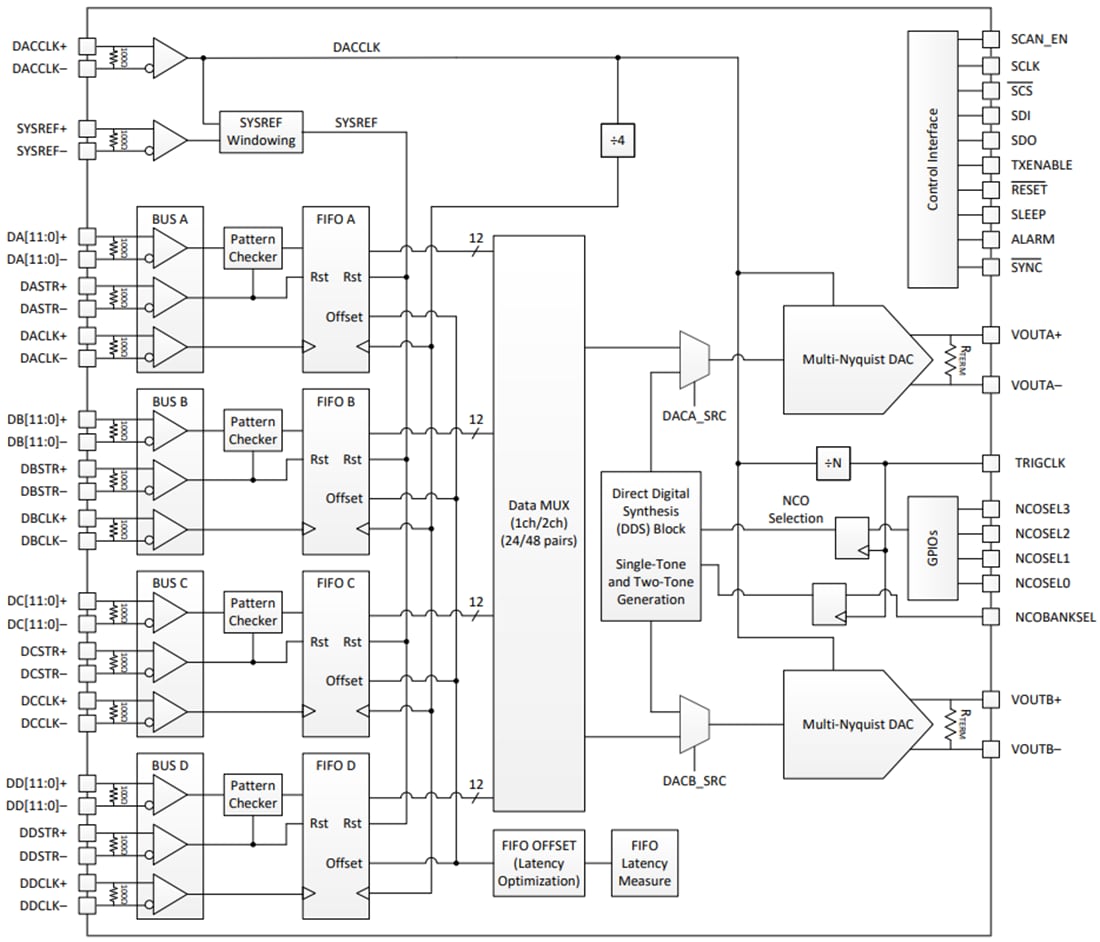
Functional Block Diagram

Block Diagram - Texas Instruments DAC12DL3200 12-Bit High-Speed DAC

Texas Instruments DAC12DL3200 12-Bit High-Speed DAC