SMARTsemi DDR4 Memory ICs

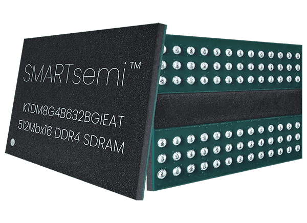
SMARTsemi DDR4 Memory ICs feature a power supply (JEDEC standard 1.2V) of VDD = 1.2V ± 5%, and VPP = 2.375V to 2.75V. The ICs have up to 8 banks (4 banks x 2 bank groups) for x 16 products. The DDR4 feature a Pseudo Open Drain (POD) interface with a Burst Length (BL) of 8 and 4 with Burst Chop (BC).

Features

  • Power supply (JEDEC standard 1.2V)
    • VDD = 1.2V ± 5%
    • VPP = 2.375V to 2.75V
  • 16 internal banks (x8)
    • 8 banks (4 banks x 2 bank groups) for x 16 product
  • Pseudo Open Drain (POD) interface
  • 8 and 4 with Burst Chop (BC) Burst Length (BL)
  • CAS Latency (CL)
    • 10,(11),12,(13),14,(15),16,(17),18,19,20,22,24
  • CAS Write Latency (CWL)
    • 9,10,11,12,14,16,18,20
  • On-Die Termination (ODT): nom. values of RZQ/7, RZQ/5 (RZQ = 240Ω)
  • Precharge auto precharge option for each burst access
  • Refresh: auto-refresh, self-refresh
  • Refresh cycles
  • Average refresh period
    • 7.8μs at 0°C ≤ TC ≤ +85°C or -40°C ≤ TC ≤ +85°C
    • 3.9μs at +85°C < TC ≤ +95°C
  • Double-data-rate architecture two data transfers per clock cycle
  • The high-speed data transfer is realized by the 8 bits prefetch pipelined architecture
  • Bi-directional differential data strobe (DQS_t and DQS_c) is transmitted/received with data for capturing data at the receiver
  • Termination Data Strobe is supported (x8 only) (TDQS_t and TDQS_c)
  • DQS is edge-aligned with data for READs; center aligned with data for WRITEs
  • Differential clock inputs (CK_t and CK_c)
  • DLL aligns DQ and DQS transitions with CK transitions
  • Commands entered on each positive CK edge; data and data mask referenced to both edges of DQS
  • Data Mask (DM) for writing data
  • Write Cyclic Redundancy Code (CRC) for DQ error detection and inform it to the controller during high-speed operation
  • Data Bus Inversion (DBI)
    • Improve the power consumption and signal integrity
    • of the memory interface (x16 product only)
  • Programmable preamble is supported by both of 1tCK and 2tCK mode
  • Command Address (CA) Parity for command/address signal error detect and inform it to a controller
  • VREFDQ training
    • VREFDQ generate inside DRAM and further trained per DRAM
  • Per DRAM Addressability (PDA)
    • Each DRAM can be set a different mode register value individually and has individual adjustments.
  • Fine granularity refresh
    • 2x, 4x mode for smaller tRFC
  • Programmable Partial Array Self-Refresh (PASR)
  • RESET_n pin for power-up sequence and reset function
  • Operating case temperature range:
    • Commercial: TC = 0°C to +95°C
    • Industrial: TC = -40°C to +95°C

SMARTsemi DDR4 Memory ICs