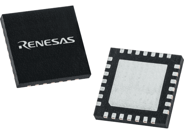
Renesas Electronics RC192x Clock Muxes

Renesas Electronics RC192x Clock Muxes are ultra-high performance clock muxes supporting PCIe Gen5 and Gen6. These muxes provide a Loss-Of-Signal (LOS) output for system monitoring and redundancy. The RC192x muxes feature Power Down Tolerance (PDT), Flexible Power Sequencing (FPS), Automatic Clock Parking (ACP), Common Clocked (CC), and Independent Reference (IR). These clock muxes drive source-terminated and double-terminated loads up to 400MHz. The RC192x clock muxes offer 2, 4, 8, or 16 Low-Power (LP) HCSL output saves up to 64 resistors. Typical applications include cloud/high-performing computing, nVME storage, networking, and accelerators.
Features

  • 2, 4, 8, or 16 Low-Power (LP) HCSL outputs save up to 64 resistors
  • 2:N or 2 x 1:N/2 modes (N is the number of outputs)
  • 85Ω or 100Ω output impedance
  • Outputs drive both source-terminated and double-terminated loads
  • Open-drain LOS output
  • FPS allows inputs and clocks to be applied before power is applied or power to be applied with no input clock
  • ACP cleanly parks outputs in a low/low state when the selected input clock is lost
  • Spread-spectrum tolerant
  • Up to 8 output enable pins
  • Selectable 4-wire Side-Band-Interface (SBI) for hardware output enable (RC19208)
  • CLKIN pins directly support HCSL or LVDS signaling levels
  • Common Clocked (CC)
  • Independent Reference (IR) with and without spread spectrum
  • 3mm x 3mm 20-VFQFPN to 6mm x 6mm 80-GQFN packages

Specifications

  • 7fs RMS PCIe Gen5 additive phase jitter
  • 4fs RMS PCIe Gen6 additive phase jitter
  • 9fs RMS DB2000Q additive phase jitter
  • 37fs RMS at 156.25MHz and 12kHz to 20MHz additive phase jitter
  • 1MHz to 400MHz operation with ACP disabled
  • 25MHz to 400MHz operation with ACP enabled

Applications

  • Cloud/high-performance computing
  • nVME storage
  • Networking
  • Accelerators

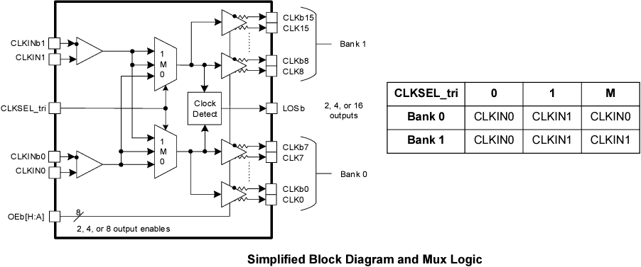
Block Diagram and Mux Logic

Block Diagram - Renesas Electronics RC192x Clock Muxes

Renesas Electronics RC192x Clock Muxes