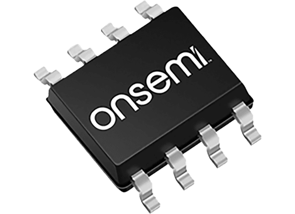
onsemi NCV8877 Non-Synchronous Boost Controller

onsemi NCV8877 Automotive Start-Stop Non-Synchronous Boost Controller is designed to supply a minimum output voltage during Start-Stop vehicle operation battery voltage sags. The controller drives an external N-channel MOSFET and uses peak current mode control with internal slope compensation. The IC incorporates an internal regulator that supplies a charge to the gate driver. Protection features include cycle-by-cycle current limiting and thermal shutdown. The onsemi SOIC-8 packaged NCV8877 offers low quiescent current sleep mode operation and boost operation initiates when the supply voltage drops below the regulation set point. The NCV8877 is enabled when the supply voltage drops below the wake-up threshold.
Features

  • Automatic enable below the wake-up threshold voltage (factory programmable)
  • Override disable function
  • Boost mode operation at the regulation set point
  • 2% output accuracy over the temperature range
  • Peak current mode control with internal slope compensation
  • Externally adjustable frequency operation
  • Wide input voltage range from 2V to 40V, 45V load dump
  • Low quiescent current in sleep mode (<12A typical)
  • Cycle-by-cycle current limit protection
  • Hiccup-Mode Overcurrent Protection (OCP)
  • Thermal Shutdown (TSD)
  • Reflow solderable
  • SOIC-8 package
  • Moisture Sensitivity Level (MSL) 1
  • Lead-free
  • NCV prefix for automotive and other applications requiring unique site and control change requirements, AEC-Q100

Specifications

  • Quiescent current
    • 14µA maximum in sleep mode, 12µA typical
    • 4.0mA maximum for no switching, 2.2mA typical
  • Oscillator
    • 153kHz to 501kHz switching frequency range
    • 89ns to 146ns minimum pulse width range
    • 81% to 85% maximum duty cycle range
    • 45mV/µs to 61mV/µs slop compensating ramp range
  • Disable
    • 1.0µA maximum pull-down current, 0.6µA typical
    • 2.0V to 5.0V input high voltage range
    • 500mV typical input high voltage hysteresis
    • 0mV to 800mV input low voltage range
  • Current sense amplifier
    • 0.9V/V to 1.1V/V low-frequency gain range
    • 2.5MHz minimum bandwidth
    • 50µA maximum ISNS input bias current, 30µA typical
    • 180mV to 220mV current limit threshold voltage range
    • 125ns maximum current limit/overcurrent protection response time, 80ns typical
    • 125% to 175% overcurrent protection threshold voltage range
  • Voltage error operational transconductance amplifier
    • 0.8mS to 1.63mS transconductance range
    • 2.0MΩ minimum output resistance
    • 2.5V maximum output voltage (minimum)
    • 80µA minimum source/sink current, 100µA typical
    • 1.1V typical clamp voltage
    • 64µs maximum switching delay, 55µs typical
  • -0.3VDC to 40VDC supply voltage range
  • 45V peak transient voltage
  • Gate driver
    • 550mA minimum sourcing current, 800mA typical
    • 480mA minimum sinking current, 600mA typical
    • 0.6V maximum driving voltage dropout, 0.3V typical
    • 35mA minimum driving voltage source current, 45mA typical
    • 0.7V maximum back drive diode voltage drop
    • 5.67V to 6.2V driving voltage range
    • 21kΩ typical pull-down resistance
  • Undervoltage lock-out (UVLO)
    • 3.54V to 4.0V threshold voltage range
    • 325mV to 570mV hysteresis range
  • Thermal shutdown
    • +160°C to +180°C threshold range
    • 10°C to 20°C hysteresis range
    • 100ns maximum delay
  • Voltage regulation
    • 6.66V to 10.20V range
    • 7.10V to 10.94V threshold IC enable range
    • 7.55V to 11.54V threshold IC disable range
  • ESD capability (all pins)
    • ≥2.0kV Human Body Model (HBM)
    • ≥200V Machine Model
  • -40°C to +150°C operating junction temperature range
  • 100°C/W package thermal resistance

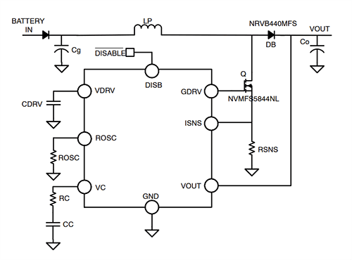
Typical Application

Application Circuit Diagram - onsemi NCV8877 Non-Synchronous Boost Controller

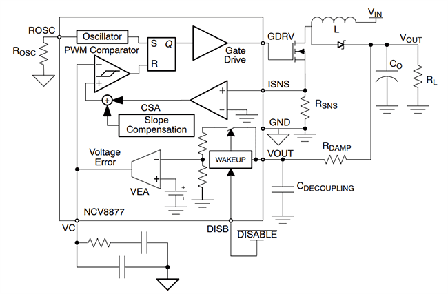
Current Mode Control Schematic

Schematic - onsemi NCV8877 Non-Synchronous Boost Controller

onsemi NCV8877 Non-Synchronous Boost Controller