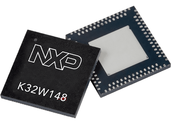
NXP Semiconductors K32W148 Multiprotocol Wireless MCUs

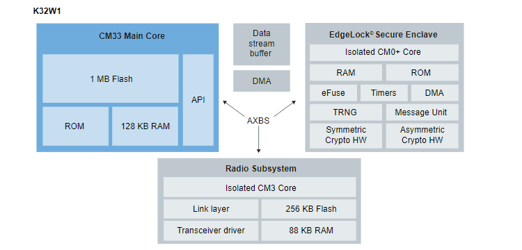
NXP Semiconductors K32W148 Multiprotocol Wireless MCUs are a low-power, highly secure, single-chip solution that integrates a BLE5.3 radio and an IEEE 802.15.4 radio supporting Thread, Matter, and Zigbee®. The K32W148 implements a tri-core architecture to isolate the connectivity, computing, and security capabilities. The multiprotocol radio is energy efficient, supporting full simultaneous dualPAN to facilitate Thread and Zigbee, and is developed for Wi-Fi coexistence. The radio is reinforced with tested software stacks for Matter, Thread, Zigbee, and BLUETOOTH® Low Energy for standalone and hosted applications to supply a range of IoT and industrial applications.

The NXP K32W148 MCUs incorporate a state-of-the-art, scalable security architecture, including Arm® TrustZone®-M, a resource domain
controller, and an isolated EdgeLock™ Secure Enclave. The device supports hardware cryptographic accelerators, random number generators, key generation, storage and management, and secure debugging. Flash memory contents can optionally be stored as encrypted data and then decrypted on-the-fly enabling protection of sensitive data and algorithms.

The K32W148 implements a flexible power-efficient architecture to extend battery life and reduce the energy footprint in IoT devices.

Features

  • Application core
    • Up to 96MHz Arm® Cortex-M33 core
    • 1MB program Flash with ECC
    • 128kB SRAM
    • Nested Vectored Interrupt Controller (NVIC)
    • Wake-up Interrupt Controller (WIC)
  • Radio Core
    • Dedicated CM3 core
    • Secure 256kB Flash for authenticated NXP 15.4 and BLUETOOTH® Low Energy controller stack firmware
    • 88kB dedicated SRAM
    • IEEE 802.15.4–2015 compliant radio
    • 101dBm 250kbps receive sensitivity
    • Improved enhanced ACK timing support in the 802.15.4 hardware
    • Dual PAN support
    • 2.4GHz BLUETOOTH Low Energy Version 5.3 upgradeable radio supporting up to 24 simultaneous hardware connections in any central/peripheral combination
    • –106dBm 125kbps long range receive sensitivity
    • –102dBm 500kbps long range receive sensitivity
    • –97.5dBm 1Mbps receive sensitivity
    • –95dBm 2Mbps receive sensitivity
    • Programmable transmit output power up to +10dBm
    • Data rates of 125kbps, 500kbps, 1Mbps, and 2Mbps
    • Modulation types: 2 Level FSK, GFSK, MSK, and GMSK
    • On-chip balun with single-ended bidirectional RF port
  • EdgeLock secure enclave
    • Secure boot and debug
    • Symmetric key encryption – AES-128/192/256 and ECB, CBC, CTR, GCM, CMAC, and CCM Modes
    • Asymmetric key encryption – ECC NIST P–192/224/256/384/521 and Curve25519
    • Key exchange algorithms – ECDH(E), SPAKE2+, JPAKE
    • Secure key generation, storage, and management
    • Flash access protection and optional encryption on-the-fly decryption using a PRINCE XEX block cipher mode
  • Low power consumption
    • Transceiver current (DC-DC buck mode, 3.3V supply)
      • Typical RX of 4.7mA
      • Typical TX at 0dBm of 4.6mA and 18.7mA at 10dBm
    • Multiple power-down modes supporting currents as low as 300nA
    • Ultra-low leakage Smart Power Switch with less than 100nA sleep current with an exit from an internal timer or GPIO
  • Clocks
    • 26MHz and 32MHz supported for BLUETOOTH LE and Generic FSK modes
    • 32.768kHz crystal oscillator, optional for BLUETOOTH LE communication
  • Operating characteristics
    • Temperature range (ambient) of –40°C to 105°C
    • Temperature range (junction) of –40°C to 125°C
    • DC/DC voltage range of 1.8V to 3.6V
    • Bypass voltage range of 1.8V to 3.6V
    • AEC-Q100 Grade 2 qualification
  • Human Machine Interface
    • 29GPIO (48HVQFN)
  • System peripherals
    • DC/DC converter supporting buck and bypass operating modes
    • Asynchronous DMA controller with per-channel access permissions (secure/non-secure)
    • Wake-up unit for power-down modes
  • Analog modules
    • 16-bit single-ended SAR analog-to-digital converter (ADC) up to 2Msps
    • Two high-speed analog comparators (CMP) with an 8-bit digital-to-analog converter (DAC)
    • 1.0V to 2.1V Voltage Reference (Vref)
    • Nested Vectored Interrupt Controller (NVIC)
    • Wake-up Interrupt Controller (WIC)
  • Timers
    • Two 6-channel 32-bit timers (TPM) with PWM capability and DMA support
    • Two 32-bit low-power timers (LPTMR) or pulse counters with compare features
    • 4-channel 32-bit low-power periodic interrupt timer (LPIT) with DMA support
    • One 56-bit timestamp timer
    • 32-bit seconds real-time counter (RTC) with 32-bit alarm and independent power supply
    • Signal frequency analyzer (SFA) provides facilities for the measurement of clock period/frequency as well as the time between triggers
  • Communication interfaces
    • Two low-power UART (LPUART) modules
    • Two low-power SPI modules and one MIPI-I3C module
    • Two low-power I2C (LPI2C) modules supporting the System Management Bus (SMBus) specification, version 2
    • One programmable FlexIO module supporting emulation of UART, I2C, SPI, Camera IF, LCD RGB, PWM/ Waveform generation
  • Packaging
    • 7mm x 7mm 48HVQFN with “Wettable” flanks
NXP Semiconductors K32W148 Multiprotocol Wireless MCUs

The K32W148 is part of the EdgeLock Assurance program, is designed to meet industry standards, and follows NXP’s security-by-design approach.
Applications

  • Industrial
    • Air Conditioning (AC)
    • Building safety
    • Building security
    • Heat metering
  • Smart city
    • Access management
  • Smart home
    • Home security and surveillance

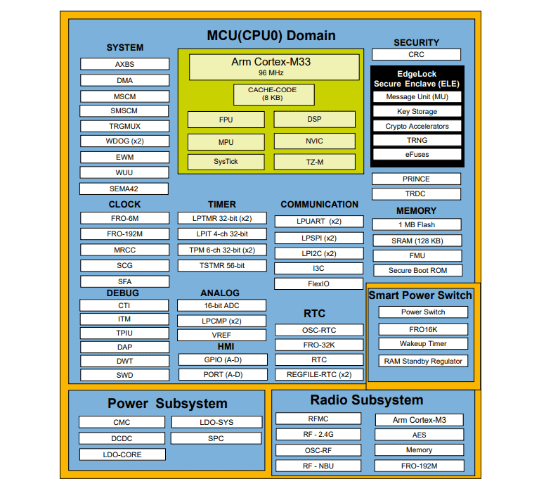
K32W1480 block diagram

Block Diagram - NXP Semiconductors K32W148 Multiprotocol Wireless MCUs

K32W148 Architecture

Application Circuit Diagram - NXP Semiconductors K32W148 Multiprotocol Wireless MCUs

NXP Semiconductors K32W148 Multiprotocol Wireless MCUs