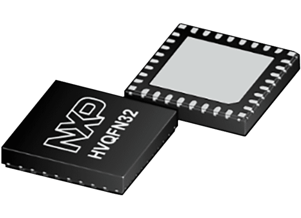
NXP Semiconductors FS2400 Fail-Safe System Basis Chips

NXP Semiconductors FS2400 Fail-Safe System Basis Chips (SBCs) offer multiple power supplies developed to support secure car access utilizing ultra-wideband (UWB), near-field communication (NFC), and BLUETOOTH® Low Energy (BLE) devices. The FS2400 family of automotive safety SBCs also conform to other small applications demanding low power and CAN FD communication.

The NXP Semiconductors FS2400 Fail-Safe SBCs support a wide range of applications, delivering a choice of output voltage settings, physical interface, and integrated system-level characteristics to address low-power and noise-sensitive applications with automotive safety integrity levels (ASIL) up to ASIL B.

The FS2400 incorporates a battery-connected switched-mode regulator (V1) and a battery-connected linear regulator (V3) to equip microcontrollers, communication devices, and others. V1 provides a high-performance switching regulator capable of operating in Pulse Frequency Modulation (PFM) mode and Force Pulse Width Modulation (FPWM) mode. The mode of operation can be changed by implementing wake pins to optimize noise management.

The FS2400 is produced in compliance with the ISO 26262:2018 standard. The device includes enhanced safety features, with fail-safe output, and becomes part of a complete safety-oriented system covering ASIL B safety integrity level. The FS2400 is available in a 5mm x 5mm, 32-Ld HVQFN package with wettable flanks.
Features

  • Power supplies
    • V1 has a high-voltage synchronous buck converter with integrated FETs. Configurable output voltage (1.9V to 5V) and switching frequency, output DC capability up to 400mA, and PFM mode for low-power on-mode operation
    • V3 has a high-voltage LDO regulator for microcontroller I/O support with a selectable output voltage between 3.3V or 5V and up to 150mA current capability
  • System support
    • One CAN FD supporting up to 5Mbps communication following ISO 11898-2:2016 and SAE J2284 standards
    • Four wake-up inputs (40V capable) WAKEx pins, HVIO1 pin, CAN FD or SPI command
    • Hardware ID detection capability
    • One high-voltage I/O with wake-up capability (40V capable) – HVIO1
    • Device control via 32-bit SPI interface, with CRC
    • Integrated long-duration timer (LDT) for system shutdown and wake-up control, programmable for up to 194 days
    • 12-channel analog multiplexer (AMUX) for system monitoring (temperature, battery voltage, internal voltages)
  • Operating range
    • 40V DC maximum input voltage
    • Low-power off mode with low sleep current and multiple wake-up sources
    • Low-power on mode with HVBUCK (V1) active, HVLDO (V3) selectable by OTP, and multiple wake-up sources
  • Functional safety
    • Developed following ISO 26262:2018 standard to fit for ASIL B applications
    • Internal monitoring circuitry with its own reference
    • Additional input for external voltage monitoring
    • Window or timeout watchdog function to monitor the MCU software failure
    • Analog built-in self-test (ABIST) on demand
    • Safety outputs (RSTB, LIMP0)
    • Safety input to monitor external IC state (ERRMON)
  • Configuration and enablement
    • HVQFN32EP offers QFN, 32-pins with exposed pad for optimized thermal management, wettable flanks, 5mm x 5mm x 0.85mm, 0.5mm pitch
    • Permanent device customization via one-time programmable (OTP) fuse memory
    • OTP emulation mode for system development and evaluation

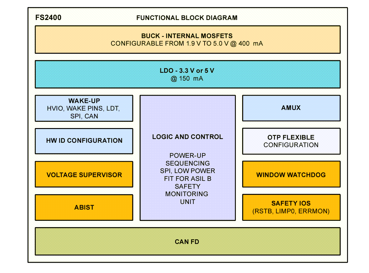
Functional Block Diagram

Block Diagram - NXP Semiconductors FS2400 Fail-Safe System Basis Chips

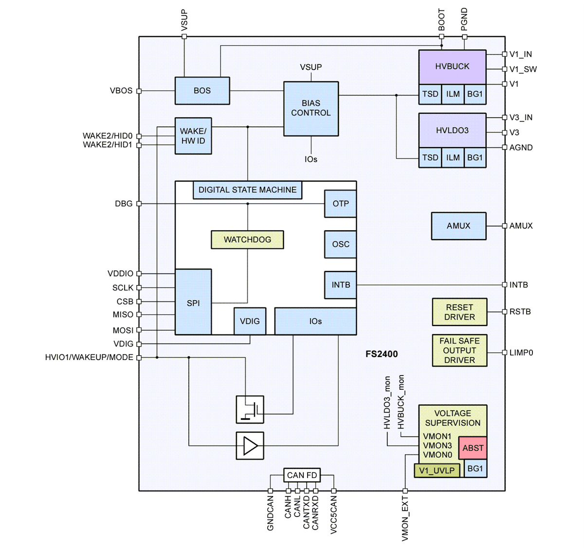
Internal block diagram

Block Diagram - NXP Semiconductors FS2400 Fail-Safe System Basis Chips

NXP Semiconductors FS2400 Fail-Safe System Basis Chips