Nexperia GAN039 CCPAK1212-Packaged Power GaN FETs

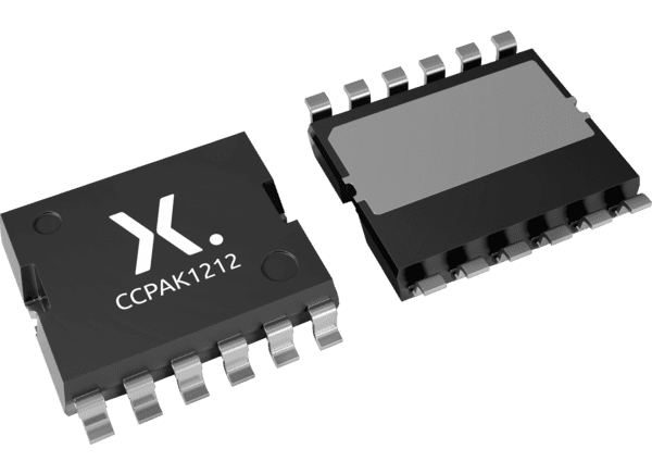
Nexperia GAN039 CCPAK1212-Packaged Power GaN FETs offer copper-clip package technology with low inductances, low switching losses, and high reliability. Wire-bond-free for optimized thermal and electrical performance, these devices provide a cascode configuration to eliminate the need for complicated drivers and controls. The surface-mount GAN039 FETs have top-side (CCPAK1212i) or traditional bottom-side (CCPAK1212) cooling to improve heat dissipation, providing added design flexibility. The CCPAK1212 and CCPAK1212i package styles feature a compact footprint of 12mm x 12mm with a low 2.5mm package height. Flexible gull-wing leads provide robust board-level reliability for extreme temperature environments.

Features

  • Compact footprint of 12mm2 with a low package height of 2.5mm
  • Ultra-low package resistance
  • High board level reliability absorbing mechanical stress during thermal cycling, unlike traditional QFN packages
  • Exposed leads allow for easy optical inspection
  • Simplified driver design
    • 0V to 12V drive voltage range
    • 4V gate threshold voltage for gate bounce immunity
  • Low body diode forward voltage for reduced losses and simplified dead-time adjustments
  • Transient over-voltage capability for increased robustness
  • Copper-clip
    • 3x times lower inductances than industry-standard packages for lower switching losses and EMI
    • Higher reliability compared to a wire-bond solution
  • 2x cooling options
    • Bottom-side cooling (CCPAK1212)
    • Top-side cooling (CCPAK1212i)
  • -55°C to +150°C junction temperature range
  • Easy solder wetting for good mechanical solder joints

Applications

  • Telecom/server titanium-grade power supplies
  • Industrial vehicle charging
  • Solar (PV) inverters
  • AC servo drives/frequency inverters
  • Battery storage/UPS inverters

Specifications

  • 650V maximum drain-source voltage
  • 60A maximum drain current
  • 240A maximum peak drain current
  • 300W maximum total power dissipation
  • 39mΩ maximum drain-source on-state resistance, 33mΩ typical
  • ±20V gate-source voltage
  • 99% power conversion efficiency
  • 5nC typical gate-drain charge
  • 30nC typical total gate charge
  • Source-drain diode
    • 150nC typical recovered charge
    • 55A maximum source current
    • 240A maximum peak source current
  • -55°C to +150°C junction temperature range

Videos

Nexperia GAN039 CCPAK1212-Packaged Power GaN FETs