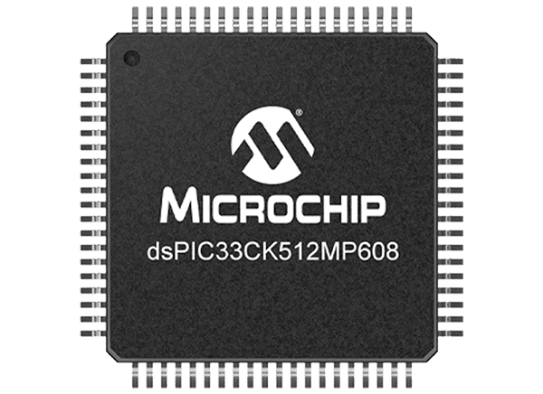
Microchip Technology dsPIC33CK512MP60x Digital Signal Controllers

Microchip Technology dsPIC33CK512MP60x 16-Bit Digital Signal Controllers (DSCs) feature a single 100 MIPS dsPIC® DSC core with an integrated Digital Signal Processor (DSP) and enhanced on-chip peripherals. The dsPIC33CK512MP60x DSCs enable the design of high-performance, precision motor control systems that are energy-efficient, quiet in operation, and provide extended motor life. These devices offer high-precision digital control of Buck, Boost, Fly-Back, Half-Bridge, Full-Bridge, LLC, and other power circuits. These features make them ideal for switched-mode AC-DC, DC-DC, UPS, and PFC power supplies. The dsPIC33CK512MP60x DSCs are also suitable for high-performance, general-purpose, and robust applications.

The Microchip Technology dsPIC33CK512MP60x DSPs include many features that help simplify functional safety certifications for ASIL-B and ASIL-C automotive applications. These devices are available in 48-pin (dsPIC33CK512MP605), 64-pin (dsPIC33CK512MP606), and 80-pin (dsPIC33CK512MP608) packages.
Features

  • dsPIC33CK DSC Core
    • Up to 512KBytes of Program Flash with ECC and Live Update (dual-partition Flash)
    • Up to 64KBytes of Data SRAM with Memory Built-in Self-Test (MBIST)
    • Modified Harvard architecture with 16-bit data and 24-bit instructions
    • Code efficient (C and Assembly) CPU architecture designed for real-time applications
    • 16x 16-bit working registers
    • 4x sets of interrupt context saving registers, including ACC and CPU status for fast interrupt handling
    • Single-cycle, mixed-sign 32-bit MUL
    • Fast 6-cycle hardware 32/16 and 16/16 DIV
    • Dual 40-bit fixed-point Accumulators (ACC) for DSP operations
    • Single-cycle MAC/MPY with dual data fetch and result write-back
    • Zero overhead looping support
  • High-Speed PWM Module
    • 8x independent PWM pairs (16 total outputs) with up to 250ps resolution
    • Dead-time insertion for rising and falling edges and dead-time compensation support
    • Clock chopping for high-frequency operation
    • Fault and current limit inputs
    • Flexible trigger configuration for ADC triggering
  • Advanced Analog Features
    • 5x 12-bit 3.5 MSPS ADC Modules, each with 4x dedicated SAR cores and 1x shared SAR core (5 S&Hs)
    • 19x, 20x, or 24x ADC input channels (depending on package)
    • 4x digital comparators for reducing CPU overhead
    • 4x oversampling filters up to 256x for increased resolution (up to 16-bits)
    • 6x analog comparators (15ns) with dedicated 12-bit DACs with hardware slope compensation
    • Up to 3x op-amps with an internal connection to ADC Module
  • Communication Interfaces
    • 3x UARTs (15Mbps) with automated protocol handling for LIN/J2602, DMX and IrDA®
    • 3x 4-wire SPI/I2S up to 40MHz with dedicated pins
    • 3x I2C Modules (up to 1Mbps) with SMBus support
    • 2x CAN Flexible Data Rate (CAN-FD) Module
    • 2x Single-Edge Nibble Transmission (SENT) Modules for sensor interfacing
    • 8x DMA channels supporting UART, SPI, ADC, CAN-FD, IC, OC, and Timer data transfers
  • Special Features
    • 4x Configurable Logic Cell (CLC) Modules with user-defined logic gate circuits
    • Programmable Pin Select (PPS) for peripheral pin function mapping
    • Parallel Master Port (PMP) for external data expansion
    • On-chip temperature sensor with direct ADC Module connection
  • Clock and Power Management
    • On-chip 8MHz Fast RC (FRC) and 32kHz Low-Power RC (LPRC) oscillators
    • Programmable PLLs with external oscillator clock sources and Reference Clock Output (REFO)
    • Fail-Safe Clock Monitor (FSCM) with 8MHz Back-up Fast RC (BFRC) oscillator
    • Low-Power management modes: Sleep, Idle, and Doze
    • Integrated Power-on Reset (POR) and Brown-Out Reset (BOR)
  • Timer/Counters/Output Compare/Input Capture
    • 24x 16-bit timer/counters (up to 12x 32-bit)
    • 14x PWM or Output Compare (OC) outputs
    • 9x Input Captures (IC) pins or internal connections from the CLC or Comparator Modules
    • 3x Quadrature Encoder Interface (QEI) Modules for optical encoder support
    • Peripheral Trigger Generator (PTG) for scheduling complex sequences
  • Debugger Development Support
    • In-Circuit and in application programming and debug support (ICSP)
    • On-chip debug trace buffer and run-time watch with 3x complex and 5x simple breakpoints
    • IEEE 1149.2 (JTAG) boundary-scan support
  • Safety Features
    • Dead-Man Timer (DMT) safety feature clocked by instruction fetches
    • WatchDog Timer (WDT)
    • CodeGuard™ security for program FLASH
    • Programmable Cyclic Redundancy Check (CRC)
    • FLASH ECC Fault Injection testing feature
    • ICSP™ write inhibit
    • Class B Safety Library, IEC 60730
  • Functional Safety Support (ISO26262)
    • ASIL-B and ASIL-C focused applications
    • FMEDA, Diagnostic Software, and Functional Safety manual available under NDA upon request from Microchip Technology
  • Functional Safety Hardware Features
    • Multiple redundant clock sources
    • I/O Port read-back
    • Analog peripherals redundancies
    • Windowed Watchdog Timer
    • RAM BIST
    • Hardware traps
    • SFR locks
    • Write protection
    • Shadow working registers
  • Operating Conditions
    • 3.0V to 3.6V, -40ºC to +125ºC, DC to 100 MIPS
    • 3.0V to 3.6V, -40ºC to +150ºC, DC to 70 MIPS
  • Package Options
    • dsPIC33CK512MP605: TQFP-48, VQFN-48 
    • dsPIC33CK512MP605: TQFP-64, VQFN-64
    • dsPIC33CK512MP605: TQFP-80

Applications

  • High-performance embedded applications
  • Motor control
  • Digital power conversion
  • Robust and safety applications
  • Industrial, automotive, and consumer applications

Resources

  • Datasheet
  • Functional Safety Quick Reference Guide

Videos

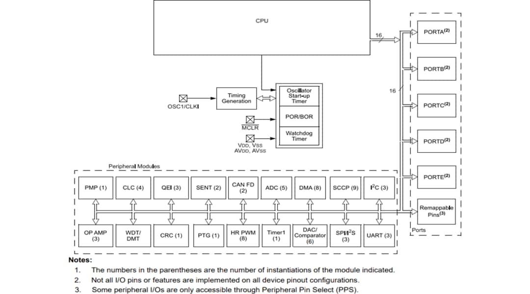
Block Diagram

Block Diagram - Microchip Technology dsPIC33CK512MP60x Digital Signal Controllers

Microchip Technology dsPIC33CK512MP60x Digital Signal Controllers