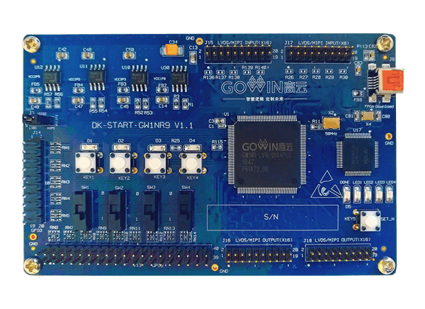
GOWIN DK-START-GW1NR9 V1.1 Development Kit

GOWIN Semiconductor DK-START-GW1NR9 V1.1 Development Kit is designed to demonstrate the LittleBee® GW1NR-9 FPGAs. The GW1NR-9 FPGAs integrate an abundant pSRAM memory chip. The GW1NR series also implements low power consumption, instant-on, low cost, non-volatile, high security, various packages, and flexible usage. The GW1NR-9 FPGAs have been optimized with low power, small size, and the thinnest package as the design goal.

The GOWIN DK-START-GW1NR9 V1.1 Development Kit offers many external interfaces, including MIPI/LVDS and GPIO. Additionally, the DK-START-GW1NR9 V1.1 Kit provides a sliding switch, button switch, LEDs, clock, reset, and other resources.
Features

  • FPGA
    • LQFP144 package
    • Up to 120 user I/O
    • Embedded flash, data not easily lost if power down
    • Abundant LUT4 resources
    • Multiple modes and capacities of B-SRAM
  • FPGA Configuration Mode
    • JTAG
    • AUTO BOOT
  • Clock resource
    • 50MHz Clock Crystal Oscillator
  • Key switch and slide switch
    • One reset button
    • Four key switches
    • Four Slide switch
  • LED
    • One power indicator (green)
    • One DONE indicator (green)
    • Four LEDs (green)
  • Memory
    • 1Mbit embedded Flash
    • 64Mbit embedded PSRAM
  • MIPI/LVDS
    • 10 pairs of LVDS differential input; 10 pairs of MIPI/LVDS differential output
  • GPIO
    • 55 I/O extended resources
  • LDO Power
    • 3.3V, 2.5V, 1.8V, and 1.2V supported

Kit Contents

  • DK-START-GW1NR9 V1.1 development board
  • USB Cable
  • Quick start guide

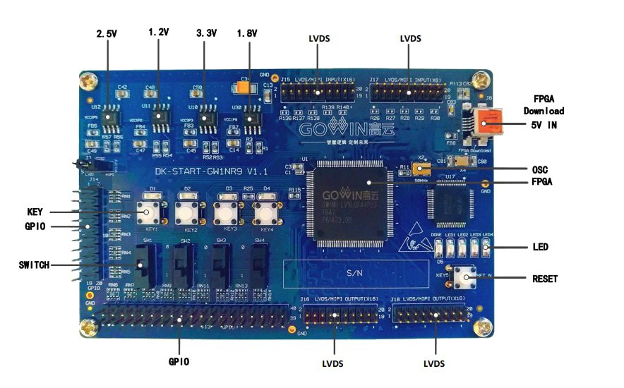
PCB Components Diagram

Location Circuit - GOWIN DK-START-GW1NR9 V1.1 Development Kit

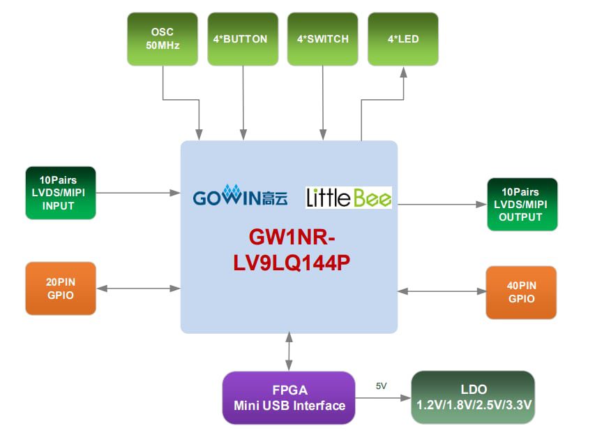
System Architecture

Block Diagram - GOWIN DK-START-GW1NR9 V1.1 Development Kit

GOWIN DK-START-GW1NR9 V1.1 Development Kit