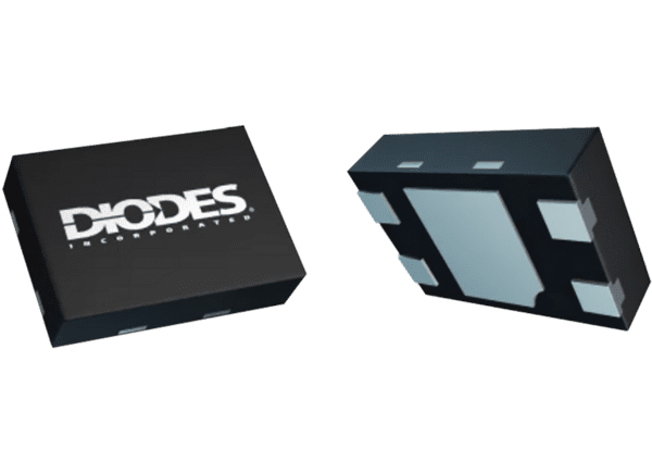
Diodes Incorporated AH139x Dual Output Unipolar Hall Effect Switch ICs

Diodes Incorporated AH139x Dual Output Unipolar Hall Effect Switch ICs offer high-sensitivity and ultra-low power in miniature packages and are specifically designed for portable/battery-powered consumer equipment, home appliances, and industrial applications. Operating over a 1.6V to 5.5V supply range and -40°C to +85°C temperature range, the AH1391 and AH1392 devices use a sleep function to give an average supply current of only 1.1μA at 1.85V. The AH139x has a 6kV ESD rating on the supply and output pins. To minimize PCB space, these ICs are packaged in small, low-profile X2-DFN1410-4 and X2-DFN1010-4 (Type B) packages.

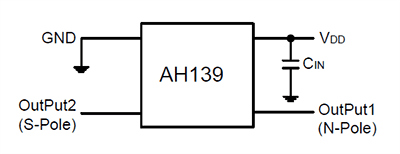
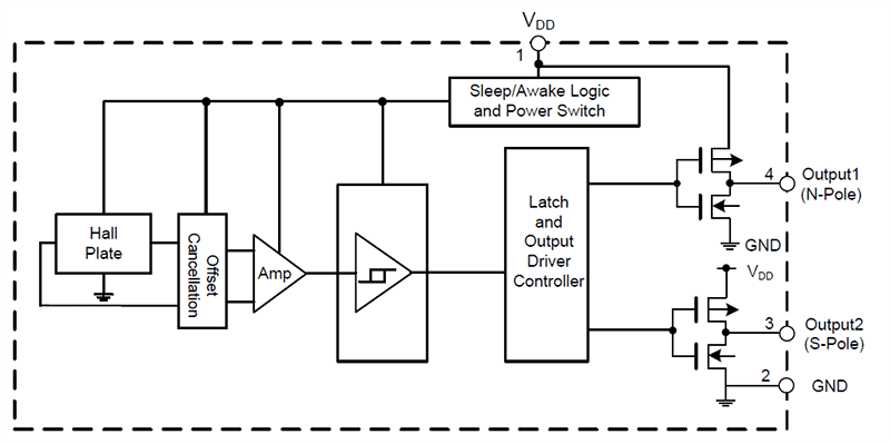
A North pole of sufficient strength will turn Output1 on, and a South pole of sufficient strength will turn on Output2. Output1 is turned on (pulled low) when the magnetic flux density (B), perpendicular to the part marking surface, falls below North field operate point BOPN (-25G typical). Output1 is held low until B rises above the North field release point BRPN (-20G typical). Similarly, Output2 will operate (pulled low) when B to the part marking surface rises above the South field operate point BOPS (25G typical) and is held low until B falls below the South field release point BRPS (20G typical).
Features

  • 2x monolithic unipolar Hall switches
    • Operation with a North Pole (Output1) to part marking surface
    • Operation with a South Pole (Output2) to part marking surface
  • 1.6V to 5.5V supply voltage
  • Micropower operation
  • Dual outputs for independent pole detection for design flexibility
  • Internal pull-up and pull-down capability
  • Good RF noise immunity
  • Chopper stabilized design
    • Superior temperature stability
    • Extremely low switch-point drift
    • Insensitive to physical stress
  • -40°C to +85°C operating temperature range
  • 6kV ESD on supply and output pins
  • Small low profile X2-DFN1410-4 and X2-DFN1010-4 (Type B) packages
  • Totally lead-free and fully RoHS compliant
  • Halogen and antimony free. “Green” device

Applications

  • Smart covers or dock detect for cellular phones and tablets
  • Position detect for digital stills, video cameras, and handheld gaming consoles
  • Doors, lids, and tray position detect switches
  • Levels, proximities, and position switches
  • Contactless switches in home appliances and industrial applications

Specifications

  • -0.3V maximum reverse supply voltage
  • 2.5mA maximum output current (source and sink)
  • Unlimited magnetic flux density
  • 230mW maximum package power dissipation
  • +150°C maximum junction temperature
  • 0.1% typical duty cycle
  • Supply currents
    • 720µA typical in IDD(AWAKE)
    • 1µA maximum, 0.36µA typical in IDD(SLEEP)
    • 3µA to 9µA maximum, 1.1µA typical for IDD(AVG)
  • 30µs to 80µs awake time range
  • 30ms to 80ms period time range

Typical Applications Circuit

Application Circuit Diagram - Diodes Incorporated AH139x Dual Output Unipolar Hall Effect Switch ICs

Functional Block Diagram

Block Diagram - Diodes Incorporated AH139x Dual Output Unipolar Hall Effect Switch ICs

Diodes Incorporated AH139x Dual Output Unipolar Hall Effect Switch ICs