- support@husseinkey.com
- livechat
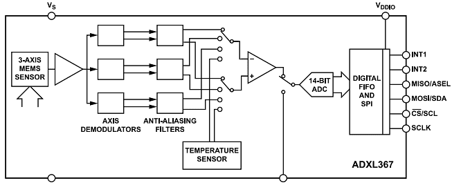
Analog Devices Inc. ADXL367 MEMS Accelerometer is an ultra-low power, 3-axis microelectromechanical systems (MEMS) accelerometer that consumes 0.89μA at a 100Hz output data rate and 180nA when in motion-triggered wake-up mode. The ADXL367 does not alias input signals by undersampling but samples the full bandwidth of the sensor at all data rates, unlike accelerometers that use power duty cycling to accomplish low power consumption. The ADI ADXL367 MEMS Accelerometer features a constant 14-bit output resolution. Meanwhile, 8-bit formatted data is delivered for more efficient single-byte transfers when a lower resolution is sufficient. 12-bit formatted data is also supported for ADXL362 design compatibility. The device offers measurement ranges of ±2g, ±4g, and ±8g are available, with a resolution of 0.25mg/LSB in the ±2g range.
The ADXL367 includes many features to enable true system-level power reduction. These features comprise of a deep multimode output first-in, first-out (FIFO), a built-in micropower temperature sensor, an internal analog-to-digital converter (ADC) for synchronous conversion of an additional analog input with interrupt capability, single-tap and double-tap detection that can operate at any output data rate with only an added 35nA of current, and a state machine to prevent false triggering. Furthermore, the ADXL367 has provisions for external control of the sampling time and an external clock.
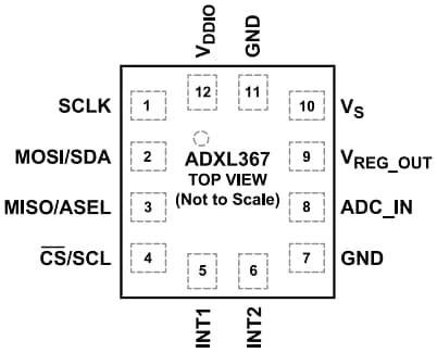
The ADXL367 operates on a wide 1.1V to 3.6V supply range and can interface, if necessary, to a host running on a separate supply voltage. The ADXL367 is housed in a 2.2mm × 2.3mm × 0.87mm package.


