- support@husseinkey.com
- livechat
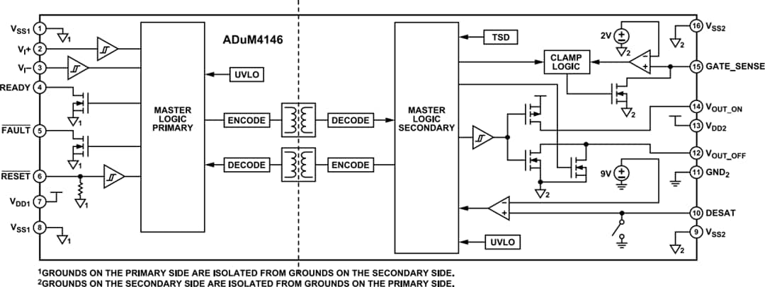
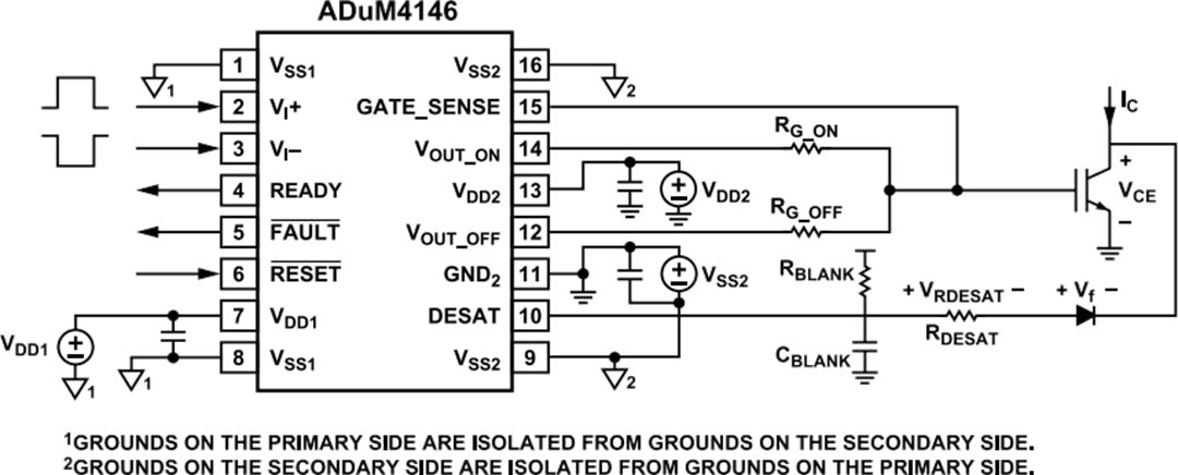
Analog Devices Inc. ADuM4146 High Voltage Isolated Bipolar Gate Driver is optimized for driving Silicon Carbide (SiC) Metal-Oxide-Semiconductor Field-Effect Transistors (MOSFETs). The ADuM4146 features iCoupler® technology, which provides isolation between the input signal and the output gate drive. The device includes a Miller clamp to provide robust SiC turn-off with a single-rail supply when the gate voltage drops to less than 2V. Operation with unipolar or bipolar secondary supplies is possible with or without the Miller clamp operation.
The ADuM4146 Gate Driver includes chip-scale transformers that provide isolated communication of control information between the high voltage and low voltage domains of the chip. Information on the status of the chip can be read back from dedicated outputs. Control of resetting the device after a fault on the secondary side is performed on the primary side of the device.
Integrated onto the ADuM4146 is a desaturation detection circuit that provides protection against high voltage short-circuit SiC operation. The desaturation protection contains noise-reducing features, such as a 300ns masking time after a switching event to mask voltage spikes due to initial turn-on. An optional internal 500μA current source allows for low device count, and the internal blanking switch allows the addition of an external current source if more noise immunity is needed.
The secondary undervoltage lockout (UVLO) is set to 14.5V (typical) for Grade A and is set to 11.5V (typical) for Grade B and Grade C with common SiC and insulated gate bipolar transistor (IGBT) levels taken into consideration.
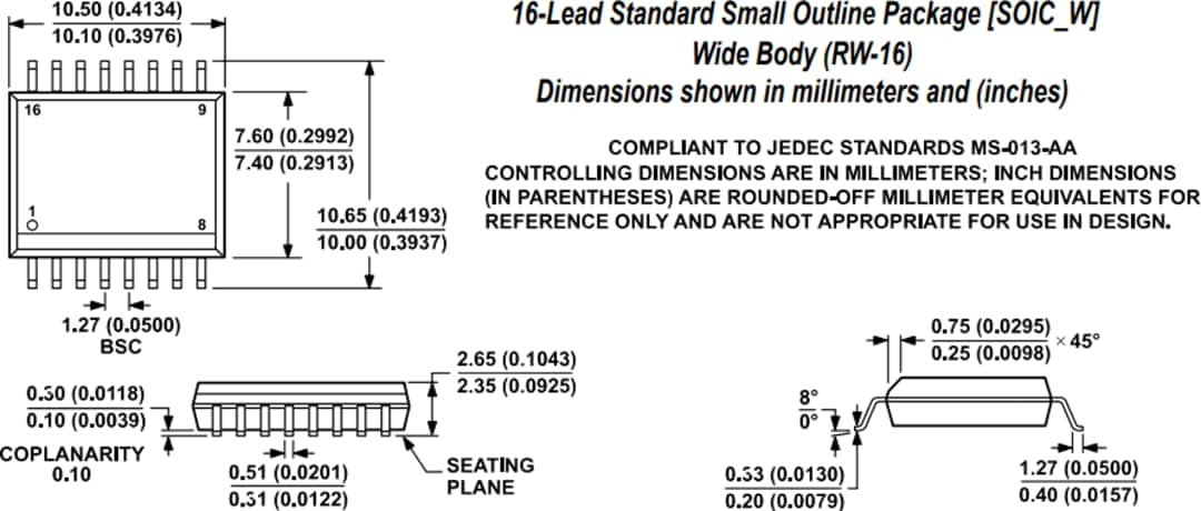
The Analog Devices Inc. ADuM4146 High Voltage Isolated Bipolar Gate Driver is offered in a 16-lead small-outline wide-body (SOIC_W) package and features a -40°C to +125°C operating temperature range.
