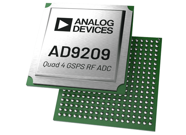
Analog Devices Inc. AD9209 Quad 12-Bit 4GSPS ADC

Analog Devices Inc. AD9209 Quad 12-Bit 4GSPS Analog-to-Digital Converter (ADC) has an on-chip wideband buffer with overload protection. This device supports applications capable of direct sampling wideband signals up to 8GHz. An on-chip, low-phase noise, phase-locked loop (PLL) clock synthesizer is available to generate the ADC sampling clock. This feature simplifies the distribution of a high-frequency clock signal’s printed circuit board (PCB). A clock output buffer is available to transmit the ADC sampling clock to other devices.

The AD9209 quad ADC cores have better code error rates (CER) than one × 10−20. Low latency, digital monitoring, and fast detection are available for AGC purposes. A flexible 192-tap programmable finite impulse response filter (PFIR) is available for digital filtering and/or equalization. The fractional delay blocks and programmable integer support compensation for analog delay mismatches.

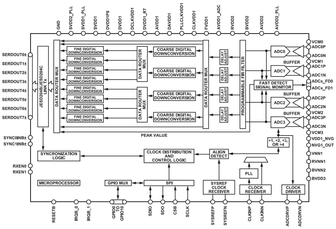
The digital signal processing (DSP) block consists of four fine DDCs and two coarse digital down converters (DDCs) per pair of ADCs. Each ADC can operate with one or two main DDC stages while supporting multi-band applications. The four additional fine DDC stages are available to support up to four bands per ADC. The 48-bit numerically controlled oscillators (NCOs) associated with each DDC support fast frequency hopping (FFH) while maintaining synchronization with up to 16 unique frequency assignments, selected via the general-purpose input and serial port interface (SPI) or output (GPIOx) pins.

The Analog Devices Inc. AD9209 supports one or two JTx links configuring for either JESD204B or JESD204C subclass operation, thus allowing for different datapaths configurations for each ADC. Multi-device synchronization is supported through the SYSREF± input pins.
Features

  • Flexible and reconfigurable common platform design
    • Supports single, dual, and quad-band
    • Datapaths and DSP blocks are fully bypassable
    • On-chip PLL with multichip synchronization
      • An external RF clock input option for off-chip PLL
      • Supports clock input frequencies up to 12GHz
  • ADC ac performance at 4GSPS
    • Differential input voltage: 1.4Vp-p
    • Noise density: −151.5dBFS/Hz
    • HD2: −69dBFS at 2.7GHz (AIN at −1dBFS)
    • HD3: −76dBFS at 2.7GHz (AIN at −1dBFS)
    • Worst other (excluding HD2 and HD3): −79dBFS at 2.7GHz
  • Versatile digital features
    • Selectable decimation filters
    • Configurable DDCs
      • Eight fine complex DDCs and four coarse complexes DDCs
      • 48-bit NCO per DDC
    • Programmable 192-tap PFIR filter for receiving equalization
      • It supports four different profile settings loaded via GPIO
    • Programmable delay per datapath
    • Receive AGC support
      • A fast detect with low latency for fast AGC control
      • Signal monitor for slow AGC control
      • Includes dedicated AGC support pins
  • Maximum ADC sample rate up to 4GSPS
    • Maximum data rate up to 4GSPS using JESD204C
    • 8GHz analog input bandwidth (−3dB)
  • Auxiliary features
    • Phase coherent fast frequency hopping
    • ADC clock driver with selectable divide ratios
    • An on-chip temperature monitoring unit
    • Flexible GPIOx pins
  • SERDES JESD204B/JESD204C interface, with eight lanes up to 24.75Gbps
    • Eight lanes per ADCs
    • Eight lanes JESD204B/JESD204C Tx (JTx)
    • Supports real or complex digital data (8-, 12-, 16-, or 24-bit)
  • 15mm × 15mm, 324-ball BGA with 0.8mm pitch

Applications

  • Wireless communications infrastructure
  • Microwave point-to-point, E-band, and 5G mm-wave
  • Broadband communications systems
  • DOCSIS 3.1 and 4.0 CMTS
  • Phased array radar and electronic warfare
  • Electronic test and measurement systems

Functional Block Diagram

Block Diagram - Analog Devices Inc. AD9209 Quad 12-Bit 4GSPS ADC

Analog Devices Inc. AD9209 Quad 12-Bit 4GSPS ADC