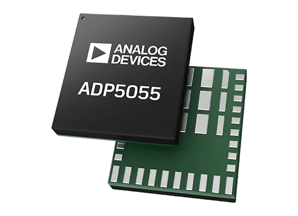
Analog Devices Inc. ADP5055 Triple Buck Regulator

Analog Devices Inc. ADP5055 Triple Buck Regulator is an integrated power solution combining three high-performance buck regulators into a compact package. The ADP5055 enables direct connection to high input voltages up to 18V with no pre-regulators. All channels on the ADP5055 integrate high-side and low-side power MOSFETs to achieve an optimized efficiency solution. Channels 1 and 2 deliver a programmable output current of 3.5A or 7.0A or provide a single output with up to 14.0A of current in parallel operation. Channel 3 delivers a programmable output current of 1.5A or 3.0A.

The switching frequency of the ADP5055 can be programmed or synchronized to an external clock. The ADP5055 contains an enable pin (ENx) on each channel for simple power-up sequencing or adjustable undervoltage lockout (UVLO) threshold.

The ADP5055 integrates a high precision 8-bit Digital-to-Analog Converter (DAC) to enable the output voltage Dynamic Voltage Scaling (DVS) via the PMBus®-compatible, 2-wire interface. The PMBus interface provides other flexible configurations, such as start-up and shutdown sequence control, individual Forced Pulse-Width Modulation or Power-Saving Mode (FPWM or PSM) selection, an output discharge switch, and a Power-Good signal.

The Analog Devices Inc. ADP5055 Triple Buck Regulator is offered in a compact 5.0mm x 5.50mm Land Grid Array (LGA) package with a -40°C to +150°C junction temperature range.
Features

  • Wide 2.75V to 18.0V input voltage range
  • 4.5V to 18.0V bias input voltage range
  • PMBus-compatible interface with configurable address 
  • FB1 voltage accuracy (default): -0.62% to +0.69% (-40°C ≤ TJ ≤ +125°C) 
  • Channel 1 and Channel 2: 7.0A synchronous buck regulator (9.4A minimum valley current-limit threshold) 
  • Channel 1 and Channel 2: 14.0A output in parallel operation 
  • Channel 3: 3.0A synchronous buck regulator (4.2A minimum valley current-limit threshold)
  • 250kHz to 2500kHz adjustable switching frequency range 
  • External compensation for fast load transient response
  • Precision enable pin with 0.615V accurate threshold
  • 8-bit precision DAC for DVS 
    • Adjustable feedback voltage range: 408mV to 790.5mV per 1.5mV step 
    • Upper and lower threshold limit setting
  • Programmable power-up and power-down sequence 
  • Selective active output discharge switch
  • Selective FPWM/PSM mode selection
  • Frequency synchronization input or output 
  • Power-Good flag on selective channels
  • UVLO, overcurrent protection, and TSD protection
  • -40°C to +150°C junction temperature range
  • 5.00mm x 5.50mm LGA-43 package

Applications

  • Small cell base stations
  • Field Programmable Gate Array (FPGA) and processor applications
  • Security and surveillance
  • Medical applications

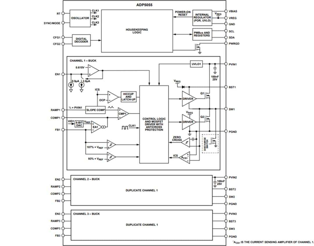
Block Diagram

Block Diagram - Analog Devices Inc. ADP5055 Triple Buck Regulator

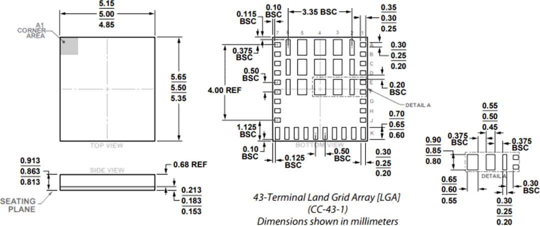
Package Outline

Mechanical Drawing - Analog Devices Inc. ADP5055 Triple Buck Regulator

Analog Devices Inc. ADP5055 Triple Buck Regulator