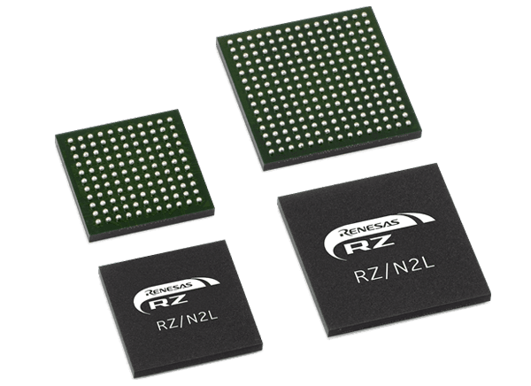
Renesas Electronics RZ/N2L Multi-Protocol Microprocessor

Renesas Electronics RZ/N2L Multi-Protocol Microprocessor is an LSI-optimized MPU that eases the implementation of Industrial Ethernet and TSN networks. The RZ/N2L MPU features an Arm® Cortex®-R52 core with a maximum operating frequency of 400MHz and a tightly coupled memory (256KB). The device integrates a 3-port Gigabit Ethernet switch that supports the next-generation network standard TSN and major Industrial Ethernet protocols such as EtherCAT, PROFINET, and EtherNet/IP. 

The RZ/N2L MPU features a rich peripheral set utilizing a Low-Latency Peripheral Port (LLPP) bus, ideal for high-precision motor control. The device is also a full Functional Safety (FuSa) solution conforming to the ISO 26262 standards. A partitioning function can separate safety and non-safety applications to avoid interference between applications, allowing developers to reduce re-certification efforts due to the separation even if one of the non-safety applications needs to be changed or re-certified.

The Renesas Electronics RZ/N2L Multi-Protocol Microprocessor is offered in 13mm x 13mm LFBGA-225 and 10mm x 10mm LFBGA-121 packages and features a -40°C to +125°C operating junction temperature range.


Features

  • 400MHz Arm Cortex-R5 core
  • Industrial Ethernet enabled
  • 3port Gigabit Ethernet switch with TSN
  • Supports multi-protocol Industrial Ethernet, including EtherCAT, PROFINET RT/IRT, and EtherNet /IP
  • PWM timer
  • ΔΣ interface
  • Easy adoption onto existing systems
  • LLPP (Low-Latency Peripheral Port) bus connects the peripherals for real-time control applications

Applications

  • Industrial robots
  • Machine tools
  • Semiconductor manufacturing equipment
  • Material handling equipment
  • Industrial network systems
  • Remote I/O
  • Sensor hubs
  • Industrial gateways

Specifications

  • On-chip 32-bit Arm Cortex-R52 processor
    • High-speed real-time control with an operating frequency of 200MHz to 400MHz
    • On-chip Single 32-bit Arm Cortex-R52 (revision r1p2)
    • Tightly coupled memory (TCM) with ECC
      • CPU0: 128KB/128KB
    • Instruction cache/data cache with ECC
      • CPU0: 16KB per cache
    • High-speed interrupt
    • The FPU supports addition, subtraction, multiplication, division, multiply-and-accumulate, and square-root operations at single-precision and double-precision.
    • The NEON, Advanced SIMD, supports integer or single precision
    • Harvard architecture with an 8-stage pipeline
    • Supports the memory protection unit (MPU)
    • Arm CoreSight architecture includes support for debugging through JTAG and SWD interfaces
  • Low power consumption
    • Standby mode and module stop function
  • On-chip SRAM
    • 1.5MB of on-chip SRAM with ECC
    • 150MHz/200MHz
  • Data transfer
    • DMAC: 8 channels x 2 units
  • Event link controller
    • Module operations can be started by event signals rather than by interrupt
    • Linked operation of modules is available even while the CPU is in the standby state
  • Reset and power supply voltage control
    • Four reset sources, including a pin reset
  • Clock functions
    • External clock/oscillator input frequency: 25MHz
    • CPU clock frequency: 200MHz to 400MHz or 150MHz to 300MHz
    • System clock frequency: 200MHz or 150MHz
    • Low-speed on-chip oscillator (LOCO): 240kHz
  • Safety functions
    • Register write protection, input clock oscillation stop detection, and CRC
    • Master Memory Protection Unit (MPU)
  • Security functions (optional)
    • Boot mode with security through encryption
    • JTAG authentication
    • Cryptologic accelerator
    • TRNG
  • Communications interfaces
    • Ethernet
      • EtherCAT slave Controller: 3 ports
      • Ethernet switch: 3 ports
      • Ethernet MAC: 1 port
    • USB 0 high-speed host/functions: 1 channel
    • CAN/CAN FD (compliant with ISO11898-1): 2 channels
    • SCI with 16-byte transmission and reception FIFOs: 6 channels
    • I2C bus interface: 3 channels for transfer at up to 400 kbps
    • SPI: 4 channels
    • xSPI: 2 channels
  • External host interfaces
    • Serial host interface (SHOSTIF)
    • Parallel host interface (PHOSTIF)
  • External address space
    • Buses for high-speed data transfer at up to 100MHz
    • Support for up to 4 CS areas
    • 8- or 16-bit bus space is selectable per area
  • Up to 35 extended-function timers
    • 16-bit x 8 + 32-bit MTU3 (9 channels), 32-bit GPT (18 channels): Input capture, output compare, PWM waveform output
    • 16-bit CMT (6 channels), 32-bit CMTW (2 channels)
  • ΔΣ interface
    • Up to 6 ΔΣ modulators are connectable
  • Trigonometric function unit
    • Simultaneous calculation of sine and cosine
    • Simultaneous calculation of arctangent and hypot_k
  • 12-bit A/D converter
    • 12 bits x 2 unit (4 channels for unit 0, 8 channels for unit 1)
  • Integrated temperature sensor for measuring temperature within the chip
  • General-purpose I/O ports
    • Input pull-up/pull-down
    • The locations of input/output functions for peripheral modules are selectable from among multiple pins
  • Operating temperature range
    • Tj = -40°C to +125°C
  • Package options
    • 13mm x 13mm LFBGA-225; 0.8mm pitch
    • 10mm x 10mm LFBGA-121; 0.8mm pitch

Videos

Block Diagram

Block Diagram - Renesas Electronics RZ/N2L Multi-Protocol Microprocessor

Renesas Electronics RZ/N2L Multi-Protocol Microprocessor