Renesas Electronics 8P34S2106A Fanout Buffer

Renesas Electronics 8P34S2106A Fanout Buffer is a high-performance, low-power, and differential dual 1:6 LVDS output 1.8V/2.5V fanout buffer. This buffer is designed for the fanout of high-frequency, very low additive phase-noise clock and data signals. The 8P34S2106A buffer supports the fail-safe operation and features two independent buffer channels, and each channel consists of six low-skew outputs. This 8P34S2106A  buffer also features high isolation between channels, 2GHz input clock frequency, and matches AC characteristics across both channels. The 8P34S2106A clock buffer is ideal for switches/routers, medical imaging, professional audio and video, 4.5G and 5G RU, and DU.
Features

  • Dual 1:6 low skew and low additive jitter LVDS fanout buffers
  • Matched AC characteristics across both channels
  • High isolation between channels
  • Low power consumption
  • Both differential CLKA, nCLKA and CLKB, nCLKB inputs accept LVDS, LVPECL, and single-ended LVCMOS levels

Specifications

  • 2GHz maximum input clock frequency
  • Output amplitudes: 350mV, 500mV, and disable (selectable)
  • 10ps typical output bank skew
  • 212ps typical output skew
  • 45fs typical (fREF = 156.25MHz, 12kHz to 20MHz) low additive phase jitter, RMS
  • 1.8V and 2.5V supply voltage range
  • Device current consumption (IDD):
    • 210mA typical: 1.8V
    • 230mA typical: 2.5V 
  • 40-VFQFPN, 6mm x 6mm x 0.9mm lead-free (RoHS 6) packaging
  • -40°C to 85°C ambient operating temperature range
  • Supports up to 105°C case temperature

Applications

  • 4.5G and 5G RU and DU
  • Switches/routers
  • Medical imaging
  • Professional audio and video

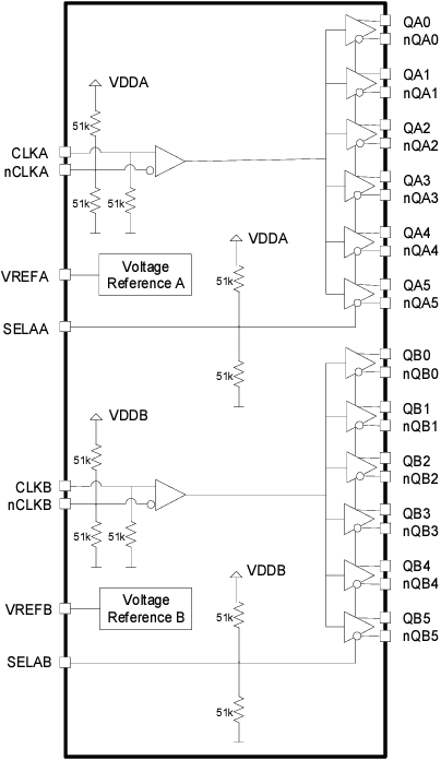
Block Diagram

Block Diagram - Renesas Electronics 8P34S2106A Fanout Buffer

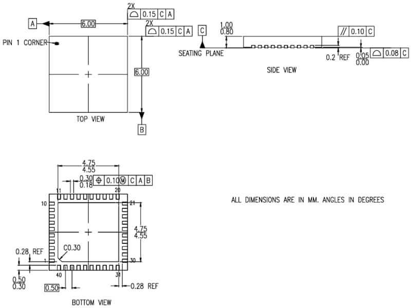
Dimension Diagram

Mechanical Drawing - Renesas Electronics 8P34S2106A Fanout Buffer

Renesas Electronics 8P34S2106A Fanout Buffer