- support@husseinkey.com
- livechat
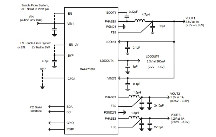
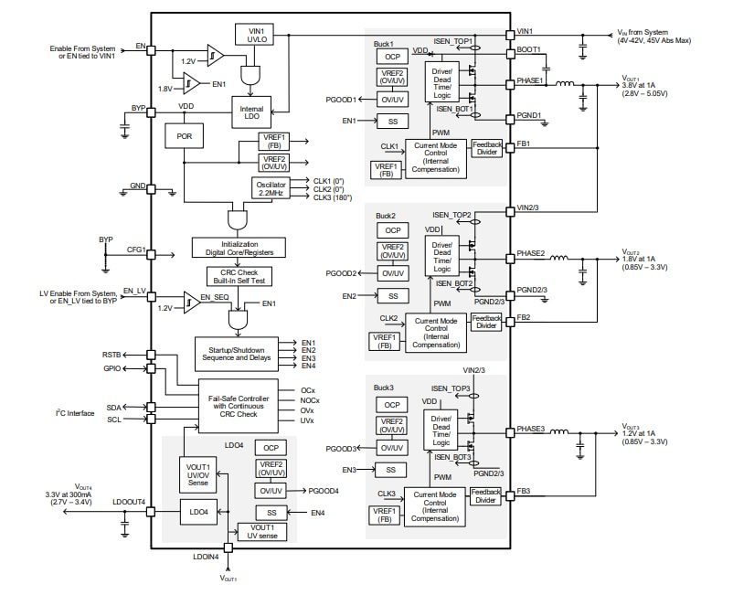
Renesas Electronics RAA271082 Automotive PMICs are adaptable multi-rail power ICs that include a primary high-voltage synchronous buck regulator, two secondary low-voltage synchronous buck regulators, and an LDO regulator. The RAA271082 delivers four overvoltage and undervoltage monitors, I2C communications, a general-purpose I/O pin, and a dedicated reset output/fault indicator.
The Renesas RAA271082 Automotive PMICs demonstrate the ASIL-D ISO-26262 development process and are designed to meet ASIL-B device metrics. The RAA271082 incorporates a second bandgap reference for the OV/UV monitors, built-in self-test at power-up, independent OV/UV monitoring, and continuous CRC error checking on internal registers and I2C communications.
The device supplies a high-density power solution and requires few external components and minimal board space. The PMICs present an extensive feature set configured using internal One-Time Programmable (OTP) memory. Almost all device options, such as each output voltage selection, power sequencing, and OV/UV thresholds, are internally configured and need no external components for selection. The regulators also deliver internal compensation. The bucks are synchronous to perform high efficiency and can operate in harsh environments requiring high ambient temperatures.
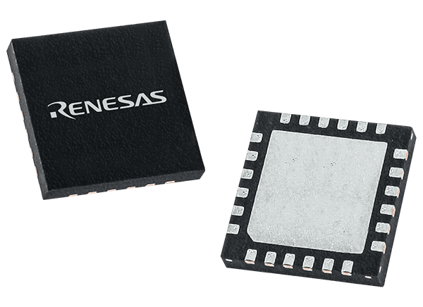
The RAA271082 is housed in a 4mm × 4mm 24-lead Step Cut QFN (SCQFN) package with an exposed pad for improved thermal performance. The device is AEC-Q100 qualified to Grade 1 and has an ambient temperature range of -40°C to +125°C and is electrically specified spanning a junction temperature range of -40°C to +150°C.
