http://www.ti.com/general/docs/suppproductinfo.tsp?distId=26&gotoUrl=https%3A%2F%2Fwww.ti.com%2Flit%2Fgpn%2Fmspm0g3105″>View Datasheet

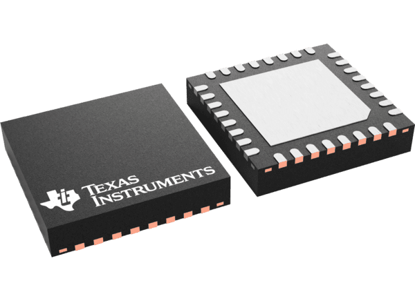
Texas Instruments MSPM0G310x Mixed-Signal Microcontrollers (MCUs)

Texas Instrument MSPM0G310x Mixed-Signal Microcontrollers (MCUs) are part of the MSP highly-integrated, 32-bit ultra-low-power MCU family based on the enhanced Arm® Cortex®-M0+ 32-bit core platform operating at up to 80MHz frequency. These cost-optimized MCUs offer high-performance analog peripheral integration, operate with supply voltages ranging from 1.62V to 3.6V, and support extended temperature ranges from -40°C to 125°C.

The Texas Instruments MSPM0G310x devices provide up to 128KB of embedded flash program memory with a built-in error correction code (ECC). These have up to 32KB SRAM with a hardware parity option. These devices incorporate a 7-channel DMA, a memory protection unit, and various high-performance analog peripherals. These peripherals include two 12-bit 4MSPS ADCs, a configurable internal shared voltage reference, and one general-purpose amplifier. These devices also offer intelligent digital peripherals such as two 16-bit advanced control timers, five general-purpose timers (with one 16-bit general-purpose timer for QEI interface, two 16-bit general-purpose timers for STANDBY mode, and one 32-bit general-purpose timer), two windowed-watchdog timers, and one RTC with alarm and calendar mode. These devices provide data integrity, encryption peripherals (CRC, TRNG, AES), and enhanced communication interfaces (four UART, two I2C, two SPI, and CAN 2.0/FD).
Features

  • Core
    • Arm 32-bit Cortex-M0+ CPU with memory protection unit, frequency up to 80MHz
  • Operating characteristics
    • Extended temperature of -40°C up to 125°C
    • 1.62V to 3.6V wide supply voltage range
  • Memories
    • Up to 128KB of flash memory with built-in error correction code (ECC)
    • Up to 32KB of SRAM with hardware parity
  • High-performance analog peripherals
    • Two simultaneous sampling 12-bit 4Msps analog-to-digital converters (ADCs) with up to 11 external channels
      • 14-bit effective resolution at 250ksps with hardware averaging
    • One general-purpose amplifier (GPAMP)
    • Configurable 1.4V or 2.5V internal shared voltage reference (VREF)
    • Integrated temperature sensor
    • Integrated supply monitor
  • Optimized low-power modes
    • RUN: 96µA/MHz (CoreMark)
    • SLEEP: 467µA at 4MHz
    • STOP: 46µA at 32kHz
    • STANDBY: 1.5µA with RTC and SRAM retention
    • SHUTDOWN: 80nA with IO wake-up capability
  • Intelligent digital peripherals
    • 7-channel DMA controller
    • Two 16-bit advanced control timers support dead band insertion and fault handling
    • Seven timers supporting up to 22 PWM channels
      • One 16-bit general-purpose timer
      • One 16-bit general-purpose timer supports QEI
      • Two 16-bit general-purpose timers support low-power operation in STANDBY mode
      • One 32-bit general-purpose timer
      • Two 16-bit advanced timers with deadband
    • Two window-watchdog timers
    • RTC with alarm and calendar mode
  • Enhanced communication interfaces
    • Four UART interfaces; one supports LIN, IrDA, DALI, Smart Card, Manchester, and three support low-power operation in STANDBY mode
    • Two I2C interfaces supporting up to FM+ (1 Mbit/s), SMBus, PMBus, and wake-up from STOP mode
    • Two SPIs, one SPI supports up to 32Mbits/s
    • One Controller Area Network (CAN) interface supports CAN 2.0 A or B and CAN-FD
  • Clock system
    • Internal 4MHz to 32MHz oscillator with up to ±3% accuracy (SYSOSC) across temperature
    • Phase-locked loop (PLL) up to 80MHz
    • Internal 32kHz oscillator (LFOSC)
    • External 4MHz to 48MHz crystal oscillator (HFXT)
    • External 32kHz crystal oscillator(LFXT)
    • External clock input
  • Data integrity and encryption
    • Cyclic redundancy checker (CRC-16, CRC-32)
    • True random number generator (TRNG)
    • AES encryption with 128 or 256-bit key
  • Flexible I/O features
    • Up to 28 GPIOs
      • Two 5V tolerant IOs
      • Two high-drive IOs with 20mA drive strength
  • Development support
    • 2-pin serial wire debug (SWD)
  • Package options
    • 32-pin VQFN
    • 28-pin VSSOP
    • 20-pin VSSOP
  • Family members
    • MSPM0G3105: 32KB flash, 16KB RAM
    • MSPM0G3106: 64KB flash, 32KB RAM
    • MSPM0G3107: 128KB flash, 32KB RAM
  • Development kits and software
    • LP-MSPM0G3507 LaunchPad™ development kit
    • MSP Software Development Kit (SDK)

Applications

  • Motor control
  • Home appliances
  • Uninterruptible power supplies and inverters
  • Electronic point-of-sale systems
  • Medical and healthcare
  • Test and measurement
  • Factory automation and control
  • Industrial transport
  • Grid infrastructure
  • Smart metering
  • Communication modules

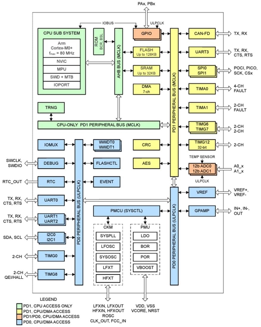
Functional Block Diagram

Block Diagram - Texas Instruments MSPM0G310x Mixed-Signal Microcontrollers (MCUs)

Texas Instruments MSPM0G310x Mixed-Signal Microcontrollers (MCUs)