http://www.ti.com/general/docs/suppproductinfo.tsp?distId=26&gotoUrl=https%3A%2F%2Fwww.ti.com%2Flit%2Fgpn%2Fam68a”>View Datasheet

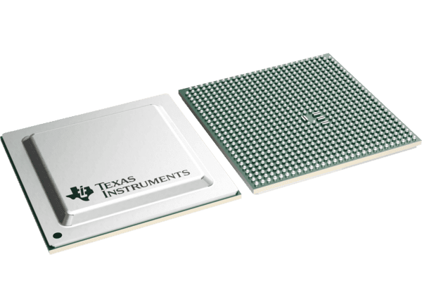
Texas Instruments AM68x 64-Bit Jacinto 8 TOPS Vision SoC Processor

Texas Instruments AM68x 64-Bit Jacinto 8 TOPS Vision SoC Processor is a scalable processor based on the evolutionary Jacinto™ 7 architecture. The series is targeted at smart vision camera applications and is built on extensive market knowledge accumulated over a decade of TI’s leadership in the vision processor market. The AM68x family is for a broad set of cost-sensitive, high-performance compute applications in factory automation, building automation, and other markets. 

The Texas Instruments AM68x series provides high-performance computing technology for both traditional and deep learning algorithms at industry-leading power/performance ratios with a high level of system integration to enable scalability and lower costs for advanced vision camera applications. Key cores include the Arm® and GPU processors for general computing, next-generation DSP with scalar and vector cores, dedicated deep learning and traditional algorithm accelerators, an integrated next-generation imaging subsystem (ISP), video codec, and isolated MCU island. All are protected by industrial-grade safety and security hardware accelerators.
Features

  • Processor cores
    • Up to dual 64-bit Arm Cortex-A72 microprocessor subsystem at up to 2GHz
      • 1MB shared L2 cache per dual-core Cortex-A72 cluster
      • 32KB L1 D-Cache and 48KB L1 I-Cache per Cortex-A72 core
    • Deep Learning Accelerator
      • Up to 8 Trillion Operations Per Second (TOPS)
    • Vision Processing Accelerators (VPAC) with Image Signal Processor (ISP) and multiple vision assist accelerators
    • Dual-core Arm Cortex-R5F MCUs at up to 1.0GHz, in general, compute partition with FFI
      • 16KB L1 D-Cache, 16KB L1 I-Cache, and 64KB L2 TCM
    • Dual-core Arm Cortex-R5F MCUs at up to 1.0GHz to support device management
      • 32K L1 D-Cache, 32K I-Cache, and 64K L2 TCM with SECDED ECC on all memories
    • Vision Processing Accelerators (VPAC) with Image Signal Processor (ISP) and multiple vision assist accelerators
      • 480MPixel/s ISP
      • Support for up to 16-bit input RAW format
      • Wide Dynamic Range (WDR), Lens Distortion Correction (LDC), Vision Imaging Subsystem (VISS), and Multi-Scalar (MSC) support
      • Output color format : 8-bits, 12-bits, and YUV 4:2:2, YUV 4:2:0, RGB, HSV/HSL
  • Multimedia
    • Display subsystem supports
      • Up to 4 displays
      • Up to two DSI 4L TX (up to 2.5K)
      • One eDP 4L
      • One DPI 24-bit RGB parallel interface
      • OLDI/LVDS (4 lanes – 2x) and 24-bit RGB parallel interface
      • Safety features such as freeze frame detection and MISR data check
    • 3D Graphics Processing Unit
      • IMG BSX-64-4, up to 800MHz
      • 50GFLOPS, 4 GTexels/s
      • > 500MTexels/s, > 8GFLOPs
      • Supports at least two composition layers
      • Supports up to 2048×1080 @60fps
      • Supports ARGB32, RGB565 and YUV formats
      • 2D graphics capable
    • OpenGL ES 3.1, Vulkan 1.2
  • Two CSI2.0 4L Camera Serial interface (CSI-Rx) Plus CSI2.- 4L Tx (CSI-Tx) with DPHY
    • MIPI CSI 1.3 Compliant + MIPI-DPHY 1.2
    • Support for 1, 2, 3, or 4 data lane modes up to 1.5Gbps
    • ECC verification/correction with CRC check + ECC on RAM
    • Virtual Channel support (up to 16)
    • Ability to write stream data directly to DDR via DMA
  • Video Encoder/Decoder
    • Support for HEVC (H.265) Main profiles at Level 5.1 High-tier
    • Support for H.264 Baseline/Main/High Profiles at Level 5.2
    • Support for up to 4K UHD resolution (3840 × 2160)
    • 4K60 H.264/H.265 Encode/Decode (up to 480MP/s)
  • Memory subsystem
    • Up to 4MB of on-chip L3 RAM with ECC and coherency
      • ECC error protection
      • Shared coherent cache
      • Supports internal DMA engine
    • Up to two External Memory Interface (EMIF) modules with ECC
      • Supports LPDDR4 memory types
      • Supports speeds up to 4266MT/s
      • Up to two 32-bit data buses with inline ECC up to 17GB/s per EMIF
    • General-Purpose Memory Controller (GPMC)
    • Up to two 512KB on-chip SRAM in MAIN domain, protected by ECC
  • Device security
    • Secure boot with secure run-time support
    • Customer programmable root key, up to RSA-4K or ECC-512
    • Embedded hardware security module
    • Crypto hardware accelerators – PKA with ECC, AES, SHA, RNG, DES, and 3DES
  • High-speed serial interfaces
    • One PCI-Express (PCIe) Gen3 controllers
      • Up to four lanes per controller
      • Gen1 (2.5GT/s), Gen2 (5.0GT/s), and Gen3 (8.0GT/s) operation with auto-negotiation
    • One USB 3.0 dual-role device (DRD) subsystem
      • Enhanced SuperSpeed Gen1 Port
      • Supports Type-C switching
      • Independently configurable as a USB host, USB peripheral, or USB DRD
    • Two CSI2.0 4L RX plus Two CSI2.04L TX
    • Two Ethernet RMII/RGMII interfaces
  • Flash memory interfaces
    • Embedded MultiMediaCard Interface (eMMC™ 5.1)
    • One Secure Digital 3.0/Secure Digital Input Output 3.0 interface (SD3.0/SDIO3.0)
    • Two simultaneous flash interfaces configured as
      • One OSPI or HyperBus™ or QSPI, and
      • One QSPI
  • Technology / Package
    • 16nm FinFET technology
    • 23mm x 23mm, 0.8mm pitch, 770-pin FCBGA (ALZ)

Applications

  • Machine vision cameras and computers
  • Smart shopping carts
  • Retail automation
  • Smart agriculture
  • Video surveillance
  • Traffic monitoring
  • Autonomous mobile robots (AMR)
  • Drones
  • Industrial transport
  • Industrial human machine interfaces (HMI)
  • Industrial PCs
  • Single board computers
  • Patient monitoring and medical devices

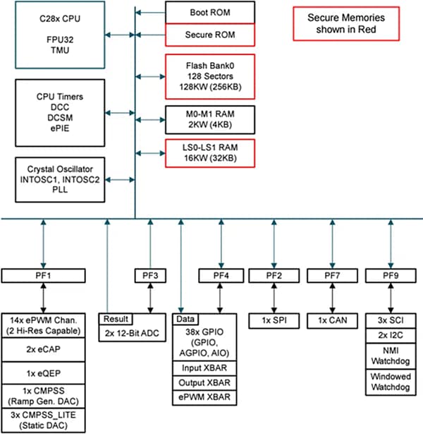
Functional Block Diagram

Block Diagram - Texas Instruments AM68x 64-Bit Jacinto 8 TOPS Vision SoC Processor

Texas Instruments AM68x 64-Bit Jacinto 8 TOPS Vision SoC Processor