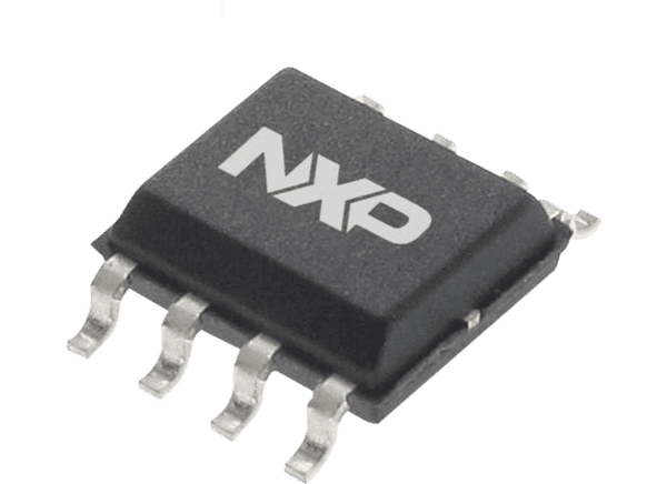
NXP Semiconductors TJA1021 LIN Transceivers

NXP Semiconductors TJA1021 LIN Transceivers interface between the LIN commander/responder protocol controller and the physical bus in a Local Interconnect Network (LIN). TJA1021 is LIN 2.0, LIN 2.1, LIN 2.2, LIN 2.2A, SAE J2602, and ISO 17987-4:2016 (12V) compliant while providing optimum ElectroMagnetic Compatibility (EMC) performance due to the LIN output wave shaping. The transceivers provide transmission speeds from 1kBd to 20kBd (maximum) and are pin-to-pin compatible with the TJA1020 and MC33662(B) series. In sleep and failure modes, power consumption is at a minimum.

Features

  • LIN 2.x/ISO 17987-4:2016 (12V)/SAE J2602 compliant
  • Baud rate up to 20kBd (/20 and B variants)
  • Very low ElectroMagnetic Emission (EME)
  • High Electromagnetic Immunity (EMI)
  • Passive behavior in an unpowered state
  • Input levels compatible with 3.3V and 5V devices
  • Integrated termination resistor for LIN responder applications
  • Wake-up source recognition (local or remote)
  • K-line compatible
  • Pin-to-pin compatible with TJA1020 and MC33662(B)
  • Available in SO8 and HVSON8 packages
  • Leadless HVSON8 package (3.0mm2) with low thermal resistance supporting Automated Optical Inspection (AOI) capability
  • Low power management, very low current consumption in Sleep mode with local and remote wake-up
  • Protections
    • High ESD robustness: ±6kV according to IEC 61000-4-2 for pins LIN, VBAT, and WAKE_N
    • Transmit data (TXD) dominant time-out function
    • Bus terminal and battery pin protected against transients in the automotive environment (ISO 7637)
    • Bus terminal short-circuit proof to battery and ground
    • Thermally protected
  • Pin-to-pin compatible with the TJA1020 and MC33662(B)

Specifications

  • Battery supply current
    • 2µA to 10µA in sleep mode
    • Standby mode
      • 150µA to 1000µA bus recessive
      • 300µA to 1200µA bus dominant
    • Normal mode
      • 300µA to 1600µA bus recessive
      • 1mA to 4mA bus dominant
  • -0.3V to +40V battery supply voltage range
  • ±40V on the LIN pin
  • ±5µA HIGH-level leakage current
  • 22.5µs maximum rise/fall time
  • -40°C to +150°C virtual junction temperature range

Block Diagram

Block Diagram - NXP Semiconductors TJA1021 LIN Transceivers

Typical Application Circuit

Application Circuit Diagram - NXP Semiconductors TJA1021 LIN Transceivers

NXP Semiconductors TJA1021 LIN Transceivers