Microchip Technology PIC16F180 Microcontrollers

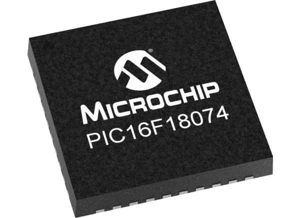
Microchip Technology PIC16F180 Microcontrollers feature an array of digital and analog peripherals for cost-sensitive sensor and real-time control needs. The Microchip Technology PIC16F180 has a memory range of 3.5KB to 28KB or speeds of up to 32MHz and is housed in 8- to 44-pin packages. The microcontrollers have a 10-bit analog-to-digital converter with computation, automated capacitive voltage divider techniques, and an 8-bit digital-to-analog converter module. Various waveform control and communication peripherals make these devices ideal for low-cost sensor and control applications.

Features

  • Core features
    • C compiler-optimized RISC architecture
    • Operating speed
      • DC 32MHz clock input
      • 125ns minimum instruction time
    • 16-level deep hardware stack
    • Low-current Power-on Reset (POR)
    • Configurable Power-up Timer (PWRT)
    • Brown-out Reset (BOR)
  • Memory
    • Up to 28KB of program flash memory
    • Up to 2KB of data SRAM memory
    • Up to 256Bytes of data EEPROM memory
    • Memory Access Partition (MAP) with program flash memory partitioned into
      • Application block
      • Boot block
      • Storage Area Flash (SAF) block
    • Programmable code protection and write protection
    • Device Information Area (DIA) stores
      • Fixed Voltage Reference (FVR) measurement data
      • Microchip Unique Identifier (MUI)
    • Device characteristics area (DCI) stores
      • Program/erase row sizes
      • Pin count details
    • Direct, indirect, and relative addressing modes
  • Digital peripherals
    • Two capture/compare/PWM (CCP) modules
      • 16-bit resolution for capture/compare modes
      • 10-bit resolution for Pulse-Width Modulator (PWM) mode
    • Three PWM
      • 10-bit resolution
    • Four Configurable Logic Cells (CLC)
      • Integrated combinational and sequential logic
    • One Complimentary Waveform Generator (CWG)
      • Rising and falling edge dead-band control
      • Full-bridge, half-bridge, and 1-channel drive
      • Multiple signal sources
      • Programmable dead band
      • Fault-shutdown input
    • One configurable 8/16-bit timer (TMR0)
    • Two 16-bit timers (TMR1/3) with gate control
    • Three 8-bit timers (TMR2/4/6) with Hardware Limit Timer (HLT)
    • One Numerically Controlled Oscillator (NCO)
      • Generates true linear frequency control and increased frequency resolution
      • Input clock up to 64MHz
    • Up to two Enhanced Universal Synchronous Asynchronous Receiver Transmitters (EUSART):
      • RS-232, RS-485, and LIN compatible
      • Auto wake-up on start
    • Up to two Host Synchronous Serial Ports (MSSP)
      • Serial Peripheral Interface (SPI) mode
    • Client select synchronization
      • Inter-integrated circuit (I2C) mode
    • 7/10-bit addressing modes
    • Peripheral Pin Select (PPS)
      • Enables pin mapping of digital I/O
    • Device I/O port features
      • Up to 35 I/O pins
      • One input-only pin
      • Individual I/O direction, open drain, input threshold, slew rate, and weak pull-up control
      • Interrupt-on-Change (IOC) on up to 25 pins
      • One external interrupt pin
  • Operating characteristics
    • Operating voltage range
      • 1.8V to 5.5V
    • Temperature range
      • Industrial -40°C to 85°C
      • Extended -40°C to 125°C
  • Power-saving functionality
    • Sleep
      • Reduce device power consumption
      • Reduce system electrical noise while performing ADC conversions
    • Low-power mode features
      • Sleep
        • < 900nA typical @ 3V/25°C (WDT enabled)
        • < 600nA typical @ 3V/25°C (WDT disabled)
      • Operating current
        • 48µA typical @ 32kHz, 3V/25°C
        • < 1mA typical @ 4MHz, 5V/25°C
  • Analog peripherals
    • Analog-to-Digital Converter with Computation (ADCC)
      • 10-bit resolution
      • Up to 35 external input channels
      • Four internal input channels
      • Internal ADC oscillator (ADCRC)
      • Operates in sleep
      • Selectable auto-conversion trigger sources
    • Charge pump module
      • Improves accuracy of analog modules at low voltages
    • 8-bit Digital-to-Analog Converter (DAC)
      • Output available on one I/O pin
      • Internal connections to ADC and comparators
    • One Comparator (CMP)
      • Up to four external inputs
      • Configurable output polarity
      • External output via peripheral pin select
    • Zero-Cross Detect (ZCD)
      • Detect when AC signal on pin crosses ground
  • Two Fixed Voltage References (FVR)
    • Selectable 1.024V, 2.048V, and 4.096V output levels
      • FVR1 internally connected to ADC
      • FVR2 internally connected to a comparator
  • Clocking structure
    • High-Precision Internal Oscillator Block (HFINTOSC)
      • Selectable frequencies up to 32MHz
      • ±2% at calibration
    • Internal 31kHz Oscillator (LFINTOSC)
    • External high-frequency clock input
      • Two External Clock (EC) power modes
    • Secondary Oscillator (SOSC)
  • Programming/debug features
    • In-Circuit Serial Programming™ (ICSP™) via two pins
    • In-Circuit Debug (ICD) with three breakpoints via two pins
    • Debug integrated on-chip

Applications

  • Cost-sensitive sensors
  • Real-time control 
  • Capacitive touch sensing
  • Waveform control
  • Communication peripherals
  • Advanced capacitive touch sensing
  • Analog-to-digital conversion
  • Digital-to-analog conversion
  • Low-power applications

Microchip Technology PIC16F180 Microcontrollers