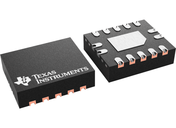
Texas Instruments SN74LV6T17/SN74LV6T17-Q1 Hex Buffers

Texas Instruments SN74LV6T17/SN74LV6T17-Q1 Hex Schmitt-Trigger Buffers contain six independent buffers with Schmitt-trigger inputs. Each gate performs the Boolean function Y = A in positive logic. The output level is referenced to the supply voltage (VCC) and supports 1.8V, 2.5V, 3.3V, and 5V CMOS levels.

The Texas Instruments SN74LV6T17/SN74LV6T17-Q1 input is designed with a lower threshold circuit to support up translation for lower voltage CMOS inputs (1.2V input to 1.8V output or 1.8V input to 3.3V output). In addition, the 5V tolerant input pins enable down translation (for example, 3.3V to 2.5V output). The SN74LV6T17-Q1 devices are AEC-Q100 qualified for automotive applications.

Features

  • Single-supply voltage translator (refer to LVxT Enhanced Input Voltage)
    • Up translation1.2V to 1.8V
      • 1.5V to 2.5V
      • 1.8V to 3.3V
      • 3.3V to 5.0V
    • Down translation
      • 5.0V, 3.3V, 2.5V to 1.8V
      • 5.0V, 3.3V to 2.5V
      • 5.0V to 3.3V
  • Available in wettable flank QFN (WBQA) package
  • Wide operating range of 1.8V to 5.5V
  • 5.5V tolerant input pins
  • Supports standard pinouts
  • Up to 150Mbps with 5V or 3.3V VCC
  • Latch-up performance exceeds 250mA per JESD 17

Applications

  • Enable or disable a digital signal
  • Controlling an indicator LED
  • Translation between communication modules and system controllers

Functional Block Diagram

Block Diagram - Texas Instruments SN74LV6T17/SN74LV6T17-Q1 Hex Buffers

Texas Instruments SN74LV6T17/SN74LV6T17-Q1 Hex Buffers