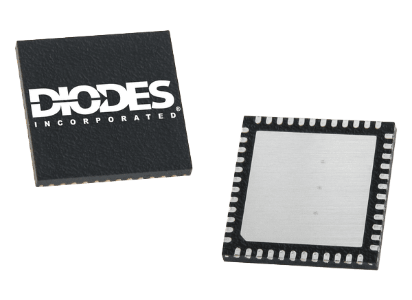
Diodes Incorporated PI6CG338Q AECQ-Grade 2 PCIe® 6.0 Clock Generator

Diodes Incorporated PI6CG338Q AECQ-Grade 2 PCIe 6.0 Clock Generator is an 8-output, very low power PCIe® (Gen 1 through Gen 6) clock generator. The PI6CG338Q uses a 25MHz crystal or CMOS reference as an input to generate the 100MHz low-power differential HCSL outputs with on-chip terminations. On-chip terminations save 32x external resistors and make the layout easier. An additional buffered reference output (provided) serves as a low-noise reference for other circuitry.

The PI6CG338Q Clock Generator uses Diodes’ proprietary PLL design to achieve a very low jitter that meets PCIe Gen 1 through Gen 6 requirements. Users can easily configure the device with various slew rate and amplitude options through the SMBUS. The device also supports selectable spread-spectrum options to reduce EMI for multiple applications.
Features

  • 3.3V supply voltage
  • 25MHz crystal/CMOS input
  • 8x differential low-power HCSL outputs with on-chip termination
  • Individual output enable
  • Reference CMOS output
  • Programmable slew rate and output amplitude for each output
  • Differential outputs blocked until the PLL is locked
  • Selectable 0%, -0.25%, or -0.5% spread on differential outputs
  • Strapping pins or SMBus for configuration
  • Differential output-to-output skew of <60ps
  • PCIe Gen 1/Gen 2/Gen 3/Gen 4/Gen 5/Gen 6 compliant
  • Very-low jitter outputs
    • PCIe 6.0 common clock (RMS) jitter of <0.04ps
    • Differential cycle-to-cycle jitter of <50ps
  • Supports Automotive Grade 2
  • Totally lead-free and fully RoHS compliant
  • Halogen- and antimony-free, green device
  • Suitable for automotive applications requiring specific change control; AEC-Q100 qualified, PPAP capable, and manufactured in IATF 16949 certified facilities
  • 48-contact, 6mm × 6mm (ZLW) packaging

Specifications

  • Power supply voltage ranges
    • 3.3135V to 3.465V
    • 1.0V to 3.465V output
    • 3.135V to 3.465V reference output
  • Power supply current ranges, all outputs active at 100MHz
    • 32mA maximum, 20mA typical
    • 25mA maximum analog, 22mA typical
    • 34mA maximum for outputs, 29mA typical
  • Power supply wake-on-LAN current
    • 1mA maximum analog, 0.5mA typical
    • 6mA maximum, 3mA typical
    • 0.1mA maximum for outputs, 0.04mA typical
  • Power supply power down current
    • 1mA maximum analog, 0.5mA typical
    • 2mA maximum, 1mA typical
    • 0.1mA maximum for outputs, 0.05mA typical
  • Input
    • 120kΩ typical internal pull-up/-down resistance
    • 8pF typical internal capacitance
    • 7nH maximum pin inductance
  • Crystal
    • Fundamental mode of operation
    • 25MHz typical frequency
    • 50Ω maximum equivalent series resistance
    • 8pF typical load capacitance
    • 7pF maximum shunt capacitance
    • 200µW maximum drive level
  • SMBus
    • 2.7V to 3.6V nominal bus voltage range
    • 4mA minimum sink current
    • 0.4V maximum output low voltage
    • 500kHz maximum operating frequency
    • 1000ns maximum rise time
    • 300ns maximum  fall time
  • 30kHz to 33kHz spread spectrum modulation frequency range
  • LVCMOS DC characteristics
    • ±5µA to ±50µA input current range
    • 20Ω typical CMOS output impedance
    • 1.5pF to 5pF input capacitance
  • LVCMOS AC characteristics
    • 25MHz typical input frequency
    • 5ns maximum rise/fall time
    • 1ms maximum clock stabilization, 0.75ms typical
  • Temperatures
    • -40°C to +105°C ambient range
    • +125°C maximum junction
  • 2000V maximum ESD protection (HBM)

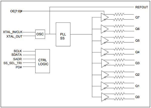
Block Diagram

Block Diagram - Diodes Incorporated PI6CG338Q AECQ-Grade 2 PCIe® 6.0 Clock Generator

Diodes Incorporated PI6CG338Q AECQ-Grade 2 PCIe® 6.0 Clock Generator