Microchip Technology PIC18-Q24 Microcontrollers

Microchip Technology PIC18-Q24 Microcontrollers are designed for sensor-interfacing, real-time control, and communication applications. The PIC18-Q24 demonstrates a Multi-Voltage I/O (MVIO) interface with multiple pins I/O powered by an alternative VDD pin, enabling these pins to operate at a different voltage domain than the rest of the microcontroller. Additionally, the PIC18-Q24 features a 10-bit analog-to-digital converter with Computation (ADCC) capable of 300ksps and an 8-bit signal routing port module to interconnect digital peripherals without using external pins.

The Microchip PIC18-Q24 Microcontrollers are available in 28-, 40-, and 48-pin devices with Enhanced Code Protection features that can be used to provide increased security and protection of user firmware and data. The Enhanced Code Protection features include Programming and Debugging Interface Disable (PDID). When enabled, this enhanced code protection feature is designed to lock out access to the programming/debugging interface and block unauthorized attempts to read, modify, or erase firmware.
Features

  • C Compiler-optimized RISC architecture
  • Operating speed:
    • DC to 64MHz clock input
    • 62.5ns minimum instruction cycle
  • Multi-Voltage I/O (MVIO):
    • Allows for operation at a voltage domain different than the normal microcontroller operating voltage
    • Provides multiple I/O pins powered by the VDDIO2 voltage domain
    • Dedicated low-voltage detect circuitry and interrupt for VDDIO2 domain
    • MVIO pins support a voltage range of 1.62V through 5.5V
  • 4x Direct Memory Access (DMA) controllers:
    • Data transfers to SFR/GPR spaces from either the program flash memory, data EEPROM, or SFR/GPR spaces
    • User-programmable source and destination sizes
    • Hardware and software-triggered data transfers
  • Vectored interrupt capability:
    • Selectable high/low priority
    • Fixed interrupt latency of 3x instruction cycles
    • Programmable vector table base address
    • Backward compatible with previous interrupt capabilities
  • 128-Level deep hardware stack
  • Low-Current Power-on Reset (POR)
  • Configurable Power-up Timer (PWRT)
  • Brown-out Reset (BOR)
  • Low-Power BOR (LPBOR) option
  • Windowed Watchdog Timer (WWDT):
    • Watchdog Reset on too long/short intervals between watchdog clear events
    • Variable prescaler and window size selection
  • Operating characteristics
    • Operating Voltage Range (VDD) of 1.8V to 5.5V
    • Multi-Voltage I/O (MVIO) range (VDDIO2) of 1.62V to 5.5V
    • High-voltage tolerant MVIO-powered pins support I2C communication down to 1.62V
  • Temperature range:
    • Industrial of -40°C to +85°C
    • Extended of -40°C to +125°C
  •  Memory
    • Up to 64KB of program flash memory
    • Up to 4KB of data SRAM memory
    • 512Bytes data EEPROM
    • Memory access partition, the program flash memory can be partitioned into:
      • Application block
      • Boot block
      • Storage Area Flash (SAF) block
    • Programmable code protection and write protection
    • Enhanced code protection
      • Programming and Debugging Interface Disable (PDID) through the ICSPDIS configuration bit
      • Storage Area Flash (SAF) one-time programmability through the SAFLOCK configuration bit
    • Device Information Area (DIA) stores:
      • Temperature indicator factory calibrated data
      • Fixed voltage reference measurement data
      • Microchip unique identifier
    • Device Characteristics Information (DCI) area stores:
      • Program/erase row sizes
      • Pin count details
      • EEPROM size
    • Direct, indirect, and relative addressing modes
  • Power-saving functionality
    • Doze: CPU and peripherals running at different cycle rates (CPU is typically slower)
    • Idle: CPU halted while peripherals operate
    • Sleep: lowest power consumption
    • Peripheral Module Disable (PMD): ability to selectively disable hardware modules to minimize active power consumption of unused peripherals
    • Low power mode features:
      • Sleep at <1µA typical at 3V
      • Operating current of 48µA at 32kHz, 3V, typical

Specifications

  • Device I/O Port:
    • 24 I/O pins including four MVIO pins powered by VDDIO2 (PIC18F24/25/26Q24)
    • 35 I/O pins including 12 MVIO pins powered by VDDIO2 (PIC18F45/46Q24)
    • 43 I/O pins including 12 MVIO pins powered by VDDIO2 (PIC18F55/56Q24)
    • MVIO pins support a voltage range of 1.62V through 5.5V
    • Individually programmable I/O direction, open-drain, slew rate, and weak pull-up control
    • Low-voltage interface on all I/O pins using LV-TTL input buffer
    • Interrupt-on-change on most pins
    • Three programmable external interrupt pins

Applications

  • Sensor-interfacing
  • Real-time control
  • Communication
  • IoT and IIoT
  • Industrial automation
  • Consumer electronics
  • Energy management applications

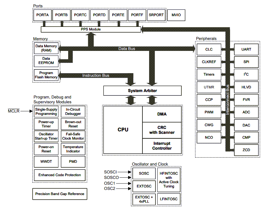
Block Diagram

Block Diagram - Microchip Technology PIC18-Q24 Microcontrollers

Family Overview

Chart - Microchip Technology PIC18-Q24 Microcontrollers

Microchip Technology PIC18-Q24 Microcontrollers