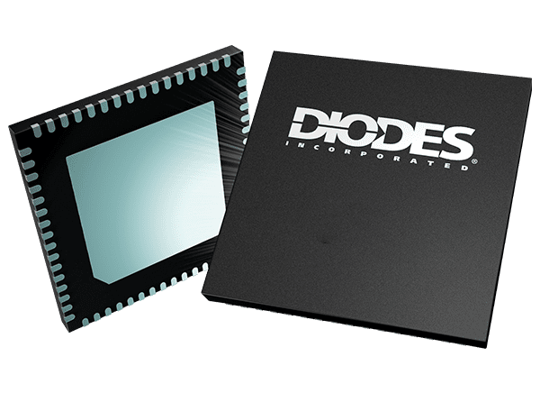
Diodes Incorporated PI6CBE33123 Low-Power PCIe® Clock Buffer

Diodes Incorporated PI6CBE33123 Low-Power PCIe® Clock Buffer is a low-power PCIe 1.0/2.0/3.0/4.0/5.0/6.0 clock buffer. PI6CBE33123 takes a reference input to fan out 12 100MHz low-power differential HCSL outputs with on-chip terminations for 33Ω output impedance. The device supports zero-delay and fanout buffer functions for various applications. An individual OE pin for each output provides easier power management. A proprietary PLL design achieves very low jitter that meets PCIe 1.0/2.0/3.0/4.0/5.0/6.0 requirements. Besides PCIe 100MHz support, this device also supports 133.33MHz via a pin.
Features

  • 12x differential low-power HCSL outputs with on-chip termination
  • 33Ω default ZOUT
  • Spread spectrum tolerant
  • Individual output enable
  • Selectable PLL bandwidths
  • Hardware/SMBus control of ZDB and fanout buffer modes
  • Up to 9x selectable SMBus addresses
  • 1MHz to 400MHz fanout buffer operation
  • 100MHz and 133.33MHz ZDB mode
  • <50ps differential output-to-output skew
  • 3.3V core supply voltage
  • -40°C to +85°C ambient/junction temperature range
  • Very low jitter outputs
    • <50ps differential cycle-to-cycle jitter
    • Fanout buffer mode additive phase jitter
      • 0.012ps PCIe 6.0 CC
      • 0.02ps DB2000Q additive jitter
    • ZDB mode phase jitter
      • RMS 0.01ps PCIe 6.0 CC
      • 0.14ps RMS QPI/UPI 11.4GB/s
      • RMS 0.15ps IF-UPI
  • 64-lead, 9mm x 9mm TQFN (ZD) package
  • Lead-free and RoHS-compliant
  • Halogen- and antimony-free, green device

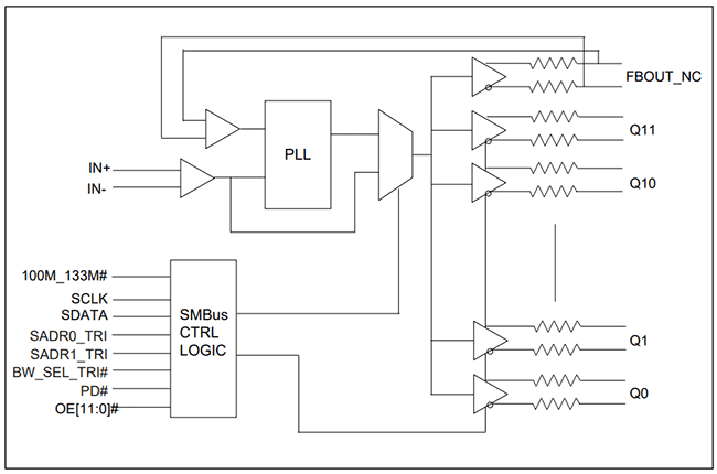
Block Diagram

Block Diagram - Diodes Incorporated PI6CBE33123 Low-Power PCIe® Clock Buffer

Diodes Incorporated PI6CBE33123 Low-Power PCIe® Clock Buffer