- support@husseinkey.com
- livechat
Infineon Technologies CoolSiC™ Automotive 750V G1 SiC Trench MOSFETs help EV makers create 11kW and 22kW bidirectional onboard chargers with increased efficiency, power density, and reliability. These devices operate reliably at high temperatures (Tj,max +175°C), featuring Infineon’s proprietary. XT die attach technology for best-in-class thermal impedance for an equivalent die size.
The CoolSiC 750V G1 technology provides very high robustness, especially against cosmic radiation, making it perfect for bus voltages >500V. Thanks to excellent immunity against spurious turn-ons, these devices can be safely driven with zero-volt VGS offstage voltage (unipolar gate driver), reducing system complexity, PCB area occupation, and BOM count. A wide gate-source voltage rating (-5V to 23V, VGS static) ensures compatibility with bipolar driving for increased design flexibility.
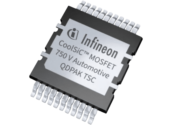
This CoolSiC™ Automotive MOSFET 750V G1 family has a very granular portfolio with the RDS(on) (at +25°C typical) from 8mΩ to 140mΩ and is available in a 7-pin D2PAK and QDPAK top side cooling (TSC) package. The JEDEC-released QDPAK TSC package helps maximize PCB space usage, doubling power density and enhancing thermal management via substrate thermal decoupling. Top-side cooled packages significantly reduce the efforts in designing the cooling infrastructure and are key to enabling the highest power densities.


