- support@husseinkey.com
- livechat
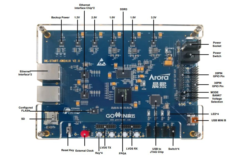
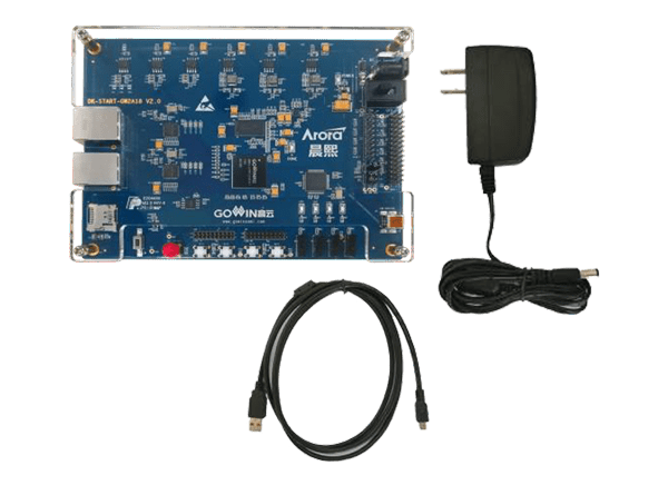
GOWIN Semiconductor DK-START-GW2A18 V2.0 Development Kit is designed to quickly and easily demonstrate the GW2A-LV18PG256 FPGA. The GW2A FPGAs offer rich internal features such as high-performance DSP, high-speed LVDS, and BSRAM memory. Along with a streamlined architecture and 55nm process, the GW2A FPGAs are suitable for high-speed and low-cost applications.
The GOWIN DK-START-GW2A18 V2.0 Development Kit is ideal for high-speed data storage, high-speed communication testing, FPGA function evaluation, hardware reliability verification, and software learning with debugging. The Development Board is equipped with a 2Gb DDR3 chip, and the maximum data rate of the 16-bit data bus is 1600MT/s. Two Gigabit Ethernet interfaces are integrated to support 10M, 100M, and 1000M Ethernet communication. Additional external interfaces include LVDS, SD cardholder, and GPIO.


