- support@husseinkey.com
- livechat
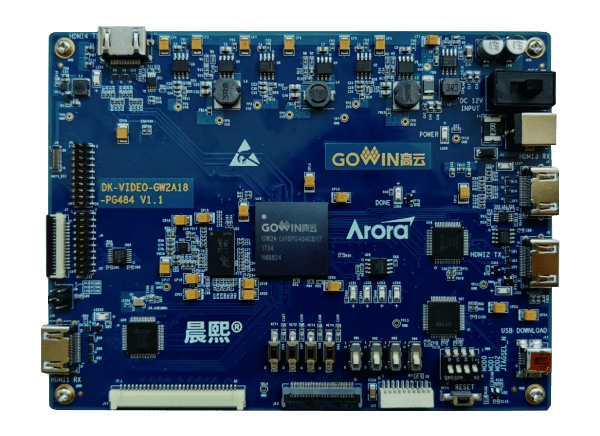
GOWIN Semiconductor DK-VIDEO-GW2A18-PG484 V1.1 Development Kit is configured to evaluate the operation of the Arora® GW2A- LV18PG484 FPGAs. The GW2A FPGAs offer a range of comprehensive features and rich internal resources like high-performance DSP resources, a high-speed LVDS interface, and abundant BSRAM memory resources.
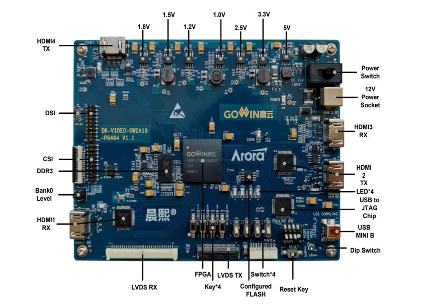
The GOWIN DK-VIDEO-GW2A18-PG484 V1.1 Development Board includes a DDR3 chip with 2Gbit storage space and 16 bits data bus width. The Board integrates four HDMI interfaces, two of which are used to receive signals (One receives signals through decoding chip, and one receives signals through FPGA IP), and the other two are used to send signals (One sends signals through decoding chip, and one sends signals through FPGA IP).
The DK-VIDEO-GW2A18-PG484 V1.1 Development Kit features abundant external interfaces, including LVDS sending interface, LVDS receiving interface, MIPI CSI, MIPI DSI, and a GPIO interface. The external Flash is used to store FPGA configuration programs.


